- 您现在的位置:买卖IC网 > PDF目录17109 > EVAL-ADUC7121QSPZ (Analog Devices Inc)BOARD EVALUATION FOR ADUC7121 PDF资料下载
参数资料
| 型号: | EVAL-ADUC7121QSPZ |
| 厂商: | Analog Devices Inc |
| 文件页数: | 21/96页 |
| 文件大小: | 0K |
| 描述: | BOARD EVALUATION FOR ADUC7121 |
| 设计资源: | ADUC7121 Gerber Files ADUC7121 Schematic |
| 标准包装: | 1 |
| 系列: | MicroConverter® ADuC7xxx |
| 类型: | MCU |
| 适用于相关产品: | ADUC7121 |
| 所含物品: | 板,CD |
第1页第2页第3页第4页第5页第6页第7页第8页第9页第10页第11页第12页第13页第14页第15页第16页第17页第18页第19页第20页当前第21页第22页第23页第24页第25页第26页第27页第28页第29页第30页第31页第32页第33页第34页第35页第36页第37页第38页第39页第40页第41页第42页第43页第44页第45页第46页第47页第48页第49页第50页第51页第52页第53页第54页第55页第56页第57页第58页第59页第60页第61页第62页第63页第64页第65页第66页第67页第68页第69页第70页第71页第72页第73页第74页第75页第76页第77页第78页第79页第80页第81页第82页第83页第84页第85页第86页第87页第88页第89页第90页第91页第92页第93页第94页第95页第96页
ADuC7121
Data Sheet
Rev. B | Page 28 of 96
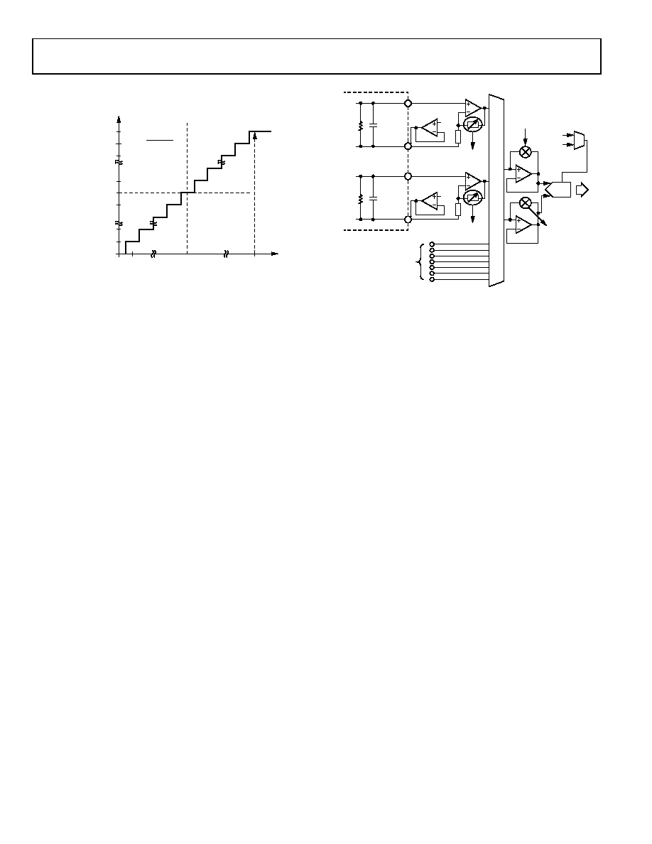
1/2 LSB, 3/2 LSBs, 5/2 LSBs, …, FS 3/2 LSBs). The ideal input/
output transfer characteristic is shown in Figure 14.
Figure 14. ADC Transfer Function in Differential Mode
PADC0x/PADC1x Pins
The PADC0x and PADC1x pins are differential input channels
to the ADC that each have a programmable gain amplifier
(PGA ) on their front ends.
An external precision resistor converts the current to voltage and
the PGA then amplifies this voltage signal with gain up to 5 by
32 steps. The intention is to compensate the variation of the
detector diode responsivity and normalize optical power read
by the ADC. The external resistor is assumed 0.1% accuracy,
5 ppm. A 1 nF capacitor is shunted with the resistor to suppress
wideband noise. Select the resistor value such that the full-scale
voltage developed on the resistor is less than AVDD 1.2 V, or
typically 1.8 V.
The PGA is designed to handle 10 mV minimum input. To
minimize noise, bypass the ADC input buffer.
PADC0N is driven by a buffer to 0.15 V to keep the PGA from
saturation when the input current drops to zero. The buffer can
be disabled by setting the ADCCON Bit 14 so that the PADC0N
pin can be connected to the ground plane as well. This is the
same for the PADC1N pin.
The ADC needs to be placed in pseudo differential mode and
assumes that the negative input is close to ground.
All of the controls are independently set through register bits
for giving maximum flexibility to the user. Typically, users need
to take the following steps:
1.
Select PADCxP and PADCxN in the ADCCP and ADCCN
registers.
2.
Optionally, bypass the ADC input buffers in
ADCCON[15:14].
3.
Set the proper gain value for the PGA in PGA_GN.
4.
Set the ADC to pseudo differential mode in
ADCCON[4:3].
5.
Start the conversion.
Figure 15. PADC0x/PADC1x ADC Input
Other Input Channels
ADuC7121 contains seven extra ADC input pins. These pins
can also be configured as differential input pairs or single-ended
inputs, or pseudo differential inputs. The buffer and ADC are
configured independently from the input channel selection. Note
that the input range of the ADC input buffer is from 0.15 V to
AVDD 0.15 V; if the input signal range exceeds this range, the
input buffer must be bypassed.
The ADuC7121 provides two pins for each thermistor input.
The negative input removes the error of the ground difference.
When selecting the thermistor input, always bypass the negative
side buffer to ensure that the amplifier is not saturated. Configure
the ADC to work in positive pseudo differential mode.
Besides these external inputs, the ADC can also select internal
inputs to monitor three power supplies: IOVDD, PVDD_IDAC0,
and PVDD_IDAC1. The voltage of the five IDAC outputs can
also be monitored by the ADC by selecting the required
channel in Register ADCCP. These internal signals are single-
ended and can select AGND/PGND/IOGND as the negative
input of the ADC via the ADCCN register.
Note that when monitoring IDAC outputs or PVDD_IDAC0,
PVDD_IDAC1, or IOVDD_MON, the buffer must be enabled
to isolate interference from ADC sampling.
An on-chip diode can also be selected to provide chip temperature
monitoring. The ADC can also select VREF and AGND as inputs
for calibration purposes.
PGA and Input Buffer
The PGA is a one stage, positive gain amplifier that is able to
accept input from 0.1 V to AVDD 1.2 V, and the output swing
should be at least 2.5 V. The gain of the PGA is from 1 to 5 with
32 linear steps. The PGA cannot be bypassed for the PADC0x
and PADC1x channels.
The input level for PGA is limited to a maximum value of
AVDD 1.2 V and minimum value of 0.1 V to ensure that the
O
UT
P
UT
CO
DE
VOLTAGE INPUT (VIN+ – VIN–)
0 1111 1111 1110
0 1111 1111 1100
0 1111 1111 1010
0 0000 0000 0001
0 0000 0000 0000
1 1111 1111 1110
1 0000 0000 0100
1 0000 0000 0010
1 0000 0000 0000
–VREF + 1LSB
+VREF – 1LSB
0LSB
1LSB =
2 × VREF
4096
SIGN
BIT
09
49
2-
0
14
PADC0_P
PADC0_N
SAR
ADC
EXTERNAL
09
49
2-
04
0
MU
X
0.15V
0.1%,
5ppm
1nF
GAIN SET BY
PGA_GN[11:6]
PADC1_P
PADC1_N
0.15V
0.1%,
5ppm
1nF
GAIN SET BY
PGA_GN[5:0]
MISCELLANEOUS
OTHER
BUFFER BYPASS
SWITCH
ADCCON[15]
BUFFER
BYPASS
SWITCH
ADCCON[14]
VREF_EXT
VREF_INT
TO
MCU
相关PDF资料 |
PDF描述 |
|---|---|
| EVAL-ADUC7126QSPZ | BOARD EVALUATION FOR ADUC7126 |
| REC5-243.3SRWZ/H4/A | CONV DC/DC 5W 9-36VIN 3.3VOUT |
| EVAL-ADUC7023QSPZ | KIT DEV FOR ADUC7023 QUICK START |
| RPS-1K-6-250/2.0-9 | HEAT SHRINK SLEEVE |
| ECM30DCWH | CONN EDGECARD 60POS DIP .156 SLD |
相关代理商/技术参数 |
参数描述 |
|---|---|
| EVALADUC7121QSPZU1 | 制造商:Analog Devices 功能描述:QUICK START DEVELOPMENT SYSTEM - Boxed Product (Development Kits) |
| EVAL-ADUC7122QSPZ | 功能描述:BOARD EVALUATION FOR ADUC7122 RoHS:是 类别:编程器,开发系统 >> 通用嵌入式开发板和套件(MCU、DSP、FPGA、CPLD等) 系列:MicroConverter® ADuC7xxx 标准包装:1 系列:PICDEM™ 类型:MCU 适用于相关产品:PIC10F206,PIC16F690,PIC16F819 所含物品:板,线缆,元件,CD,PICkit 编程器 产品目录页面:659 (CN2011-ZH PDF) |
| EVAL-ADUC7124QSPZ | 功能描述:BOARD EVALUATION FOR ADUC7124 RoHS:是 类别:编程器,开发系统 >> 通用嵌入式开发板和套件(MCU、DSP、FPGA、CPLD等) 系列:MicroConverter® ADuC7xxx 标准包装:1 系列:PICDEM™ 类型:MCU 适用于相关产品:PIC10F206,PIC16F690,PIC16F819 所含物品:板,线缆,元件,CD,PICkit 编程器 产品目录页面:659 (CN2011-ZH PDF) |
| EVAL-ADUC7126QSPZ | 功能描述:BOARD EVALUATION FOR ADUC7126 RoHS:是 类别:编程器,开发系统 >> 通用嵌入式开发板和套件(MCU、DSP、FPGA、CPLD等) 系列:MicroConverter® ADuC7xxx 标准包装:1 系列:PICDEM™ 类型:MCU 适用于相关产品:PIC10F206,PIC16F690,PIC16F819 所含物品:板,线缆,元件,CD,PICkit 编程器 产品目录页面:659 (CN2011-ZH PDF) |
| EVAL-ADUC7128QSPZ | 功能描述:KIT DEV FOR ADUC7128 RoHS:是 类别:编程器,开发系统 >> 通用嵌入式开发板和套件(MCU、DSP、FPGA、CPLD等) 系列:QuickStart™ PLUS 套件 产品培训模块:Blackfin® Processor Core Architecture Overview Blackfin® Device Drivers Blackfin® Optimizations for Performance and Power Consumption Blackfin® System Services 特色产品:Blackfin? BF50x Series Processors 标准包装:1 系列:Blackfin® 类型:DSP 适用于相关产品:ADSP-BF548 所含物品:板,软件,4x4 键盘,光学拨轮,QVGA 触摸屏 LCD 和 40G 硬盘 配用:ADZS-BFBLUET-EZEXT-ND - EZ-EXTENDER DAUGHTERBOARDADZS-BFLLCD-EZEXT-ND - BOARD EXT LANDSCAP LCD INTERFACE 相关产品:ADSP-BF542BBCZ-4A-ND - IC DSP 16BIT 400MHZ 400CSBGAADSP-BF544MBBCZ-5M-ND - IC DSP 16BIT 533MHZ MDDR 400CBGAADSP-BF542MBBCZ-5M-ND - IC DSP 16BIT 533MHZ MDDR 400CBGAADSP-BF542KBCZ-6A-ND - IC DSP 16BIT 600MHZ 400CSBGAADSP-BF547MBBCZ-5M-ND - IC DSP 16BIT 533MHZ MDDR 400CBGAADSP-BF548BBCZ-5A-ND - IC DSP 16BIT 533MHZ 400CSBGAADSP-BF547BBCZ-5A-ND - IC DSP 16BIT 533MHZ 400CSBGAADSP-BF544BBCZ-5A-ND - IC DSP 16BIT 533MHZ 400CSBGAADSP-BF542BBCZ-5A-ND - IC DSP 16BIT 533MHZ 400CSBGA |
发布紧急采购,3分钟左右您将得到回复。