- 您现在的位置:买卖IC网 > PDF目录17109 > EVAL-ADUC7124QSPZ (Analog Devices Inc)BOARD EVALUATION FOR ADUC7124 PDF资料下载
参数资料
| 型号: | EVAL-ADUC7124QSPZ |
| 厂商: | Analog Devices Inc |
| 文件页数: | 56/108页 |
| 文件大小: | 0K |
| 描述: | BOARD EVALUATION FOR ADUC7124 |
| 设计资源: | EVAL-ADUC7124 Schematic ADUC7124 Eval Brd Gerber Files |
| 标准包装: | 1 |
| 系列: | MicroConverter® ADuC7xxx |
| 类型: | MCU |
| 适用于相关产品: | ADUC7124 |
| 所含物品: | 板 |
第1页第2页第3页第4页第5页第6页第7页第8页第9页第10页第11页第12页第13页第14页第15页第16页第17页第18页第19页第20页第21页第22页第23页第24页第25页第26页第27页第28页第29页第30页第31页第32页第33页第34页第35页第36页第37页第38页第39页第40页第41页第42页第43页第44页第45页第46页第47页第48页第49页第50页第51页第52页第53页第54页第55页当前第56页第57页第58页第59页第60页第61页第62页第63页第64页第65页第66页第67页第68页第69页第70页第71页第72页第73页第74页第75页第76页第77页第78页第79页第80页第81页第82页第83页第84页第85页第86页第87页第88页第89页第90页第91页第92页第93页第94页第95页第96页第97页第98页第99页第100页第101页第102页第103页第104页第105页第106页第107页第108页
Data Sheet
ADuC7124/ADuC7126
Rev. C | Page 51 of 108
OTHER ANALOG PERIPHERALS
DAC
The ADuC7124/ADuC7126 incorporate two, or four, 12-bit
voltage output DACs on chip, depending on the model. Each
DAC has a rail-to-rail voltage output buffer capable of driving
5 kΩ/100 pF.
Each DAC has three selectable ranges: 0 V to VREF (internal
band gap 2.5 V reference), 0 V to DACREF, and 0 V to AVDD.
DACREF is equivalent to an external reference for the DAC.
The signal range is 0 V to AVDD.
MMRs Interface
Each DAC is independently configurable through a control
register and a data register. These two registers are identical for
the four DACs. Only DAC0CON (see Table 63) and DAC0DAT
(see Table 65) are described in detail in this section.
Table 62. DACxCON Registers
Name
Address
Default Value
Access
DAC0CON
0xFFFF0600
0x00
R/W
DAC1CON
0xFFFF0608
0x00
R/W
DAC2CON
0xFFFF0610
0x00
R/W
DAC3CON
0xFFFF0618
0x00
R/W
Table 63. DAC0CON MMR Bit Descriptions
Bit
Value
Name
Description
[7:6]
Reserved.
5
DACCLK
DAC update rate.
Set by the user to update the DAC
using Timer1.
Cleared by the user to update the
DAC using HCLK (core clock).
4
DACCLR
DAC clear bit.
Set by the user to enable normal
DAC operation.
Cleared by the user to reset the data
register of the DAC to 0.
3
Reserved. This bit should be left at 0.
2
Reserved. This bit should be left at 0.
[1:0]
DAC range bits.
00
Power-down mode. The DAC output
is in tristate.
01
0 V to DACREF range.
10
0 V to VREF (2.5 V) range.
11
0 V to AVDD range.
Table 64. DACxDAT Registers
Name
Address
Default Value
Access
DAC0DAT
0xFFFF0604
0x00000000
R/W
DAC1DAT
0xFFFF060C
0x00000000
R/W
DAC2DAT
0xFFFF0614
0x00000000
R/W
DAC3DAT
0xFFFF061C
0x00000000
R/W
Table 65. DAC0DAT MMR Bit Descriptions
Bit
Description
[31:28]
Reserved.
[27:16]
12-bit data for DAC0.
[15:0]
Reserved.
Using the DACs
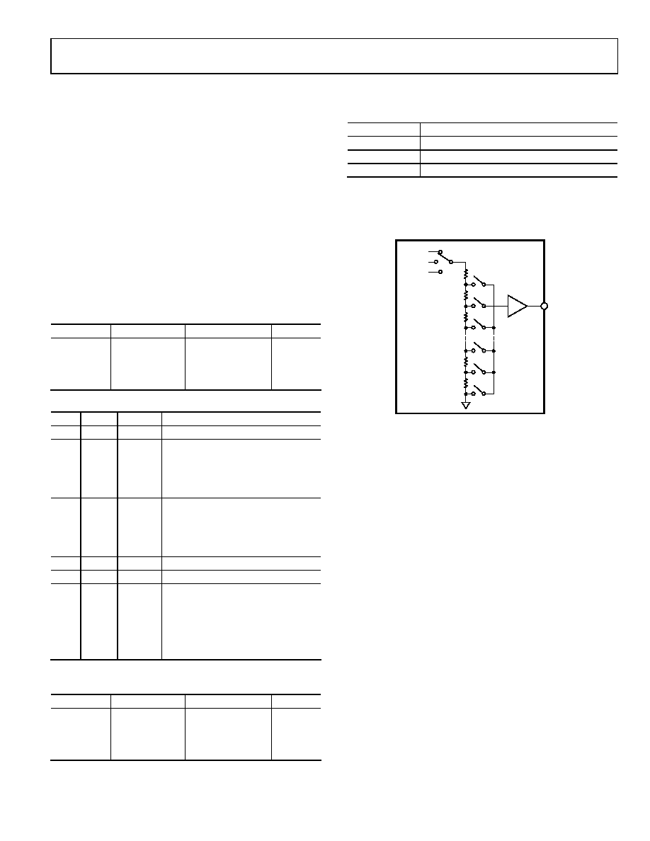
The on-chip DAC architecture consists of a DAC resistor string
followed by an output buffer amplifier. The functional equivalent
is shown in Figure 41.
09
12
3-
02
3
R
DAC0
VREF
AVDD
DACREF
Figure 41. DAC Structure
As illustrated in Figure 41, the reference source for each DAC is
user selectable in software. It can be either AVDD, VREF, or DACREF.
In 0 V-to-AVDD mode, the DAC output transfer function spans
from 0 V to the voltage at the AVDD pin. In 0 V-to-DACREF mode,
the DAC output transfer function spans from 0 V to the voltage at
the DACREF pin. In 0 V-to-VREF mode, the DAC output transfer
function spans from 0 V to the internal 2.5 V reference, VREF.
The DAC output buffer amplifier features a true, rail-to-rail
output stage implementation. This means that, when unloaded,
each output is capable of swinging to within less than 5 mV of
both AVDD and ground. Moreover, the DAC linearity specification
(when driving a 5 kΩ resistive load to ground) is guaranteed
through the full transfer function except the 0 to 100 codes,
and, in 0 V-to-AVDD mode only, Code 3995 to Code 4095.
Linearity degradation near ground and VDD is caused by satu-
ration of the output amplifier, and a general representation of its
effects (neglecting offset and gain error) is illustrated in Figure 42.
The dotted line in Figure 42 indicates the ideal transfer function,
and the solid line represents what the transfer function may
look like with endpoint nonlinearities due to saturation of the
output amplifier. Note that Figure 42 represents a transfer function
in 0 V-to-AVDD mode only. In 0 V-to-VREF or 0 V-to-DACREF
mode (with VREF < AVDD or DACREF < AVDD), the lower nonlinear-
ity is similar. However, the upper portion of the transfer function
follows the ideal line right to the end (VREF in this case, not AVDD),
showing no signs of endpoint linearity errors.
相关PDF资料 |
PDF描述 |
|---|---|
| ECM30DCWN | CONN EDGECARD 60POS DIP .156 SLD |
| EVAL-ADUC7121QSPZ | BOARD EVALUATION FOR ADUC7121 |
| EVAL-ADUC7126QSPZ | BOARD EVALUATION FOR ADUC7126 |
| REC5-243.3SRWZ/H4/A | CONV DC/DC 5W 9-36VIN 3.3VOUT |
| EVAL-ADUC7023QSPZ | KIT DEV FOR ADUC7023 QUICK START |
相关代理商/技术参数 |
参数描述 |
|---|---|
| EVAL-ADUC7126QSPZ | 功能描述:BOARD EVALUATION FOR ADUC7126 RoHS:是 类别:编程器,开发系统 >> 通用嵌入式开发板和套件(MCU、DSP、FPGA、CPLD等) 系列:MicroConverter® ADuC7xxx 标准包装:1 系列:PICDEM™ 类型:MCU 适用于相关产品:PIC10F206,PIC16F690,PIC16F819 所含物品:板,线缆,元件,CD,PICkit 编程器 产品目录页面:659 (CN2011-ZH PDF) |
| EVAL-ADUC7128QSPZ | 功能描述:KIT DEV FOR ADUC7128 RoHS:是 类别:编程器,开发系统 >> 通用嵌入式开发板和套件(MCU、DSP、FPGA、CPLD等) 系列:QuickStart™ PLUS 套件 产品培训模块:Blackfin® Processor Core Architecture Overview Blackfin® Device Drivers Blackfin® Optimizations for Performance and Power Consumption Blackfin® System Services 特色产品:Blackfin? BF50x Series Processors 标准包装:1 系列:Blackfin® 类型:DSP 适用于相关产品:ADSP-BF548 所含物品:板,软件,4x4 键盘,光学拨轮,QVGA 触摸屏 LCD 和 40G 硬盘 配用:ADZS-BFBLUET-EZEXT-ND - EZ-EXTENDER DAUGHTERBOARDADZS-BFLLCD-EZEXT-ND - BOARD EXT LANDSCAP LCD INTERFACE 相关产品:ADSP-BF542BBCZ-4A-ND - IC DSP 16BIT 400MHZ 400CSBGAADSP-BF544MBBCZ-5M-ND - IC DSP 16BIT 533MHZ MDDR 400CBGAADSP-BF542MBBCZ-5M-ND - IC DSP 16BIT 533MHZ MDDR 400CBGAADSP-BF542KBCZ-6A-ND - IC DSP 16BIT 600MHZ 400CSBGAADSP-BF547MBBCZ-5M-ND - IC DSP 16BIT 533MHZ MDDR 400CBGAADSP-BF548BBCZ-5A-ND - IC DSP 16BIT 533MHZ 400CSBGAADSP-BF547BBCZ-5A-ND - IC DSP 16BIT 533MHZ 400CSBGAADSP-BF544BBCZ-5A-ND - IC DSP 16BIT 533MHZ 400CSBGAADSP-BF542BBCZ-5A-ND - IC DSP 16BIT 533MHZ 400CSBGA |
| EVAL-ADUC7128QSPZ2 | 制造商:AD 制造商全称:Analog Devices 功能描述:Precision Analog Microcontroller ARM7TDMI MCU with 12-Bit ADC and DDS DAC |
| EVAL-ADUC7129QSPZ | 制造商:Analog Devices 功能描述:- Bulk |
| EVAL-ADUC812QS | 制造商:Analog Devices 功能描述:DEVELOPMENT KIT SYSTEM |
发布紧急采购,3分钟左右您将得到回复。