- 您现在的位置:买卖IC网 > PDF目录17109 > EVAL-ADUC7124QSPZ (Analog Devices Inc)BOARD EVALUATION FOR ADUC7124 PDF资料下载
参数资料
| 型号: | EVAL-ADUC7124QSPZ |
| 厂商: | Analog Devices Inc |
| 文件页数: | 41/108页 |
| 文件大小: | 0K |
| 描述: | BOARD EVALUATION FOR ADUC7124 |
| 设计资源: | EVAL-ADUC7124 Schematic ADUC7124 Eval Brd Gerber Files |
| 标准包装: | 1 |
| 系列: | MicroConverter® ADuC7xxx |
| 类型: | MCU |
| 适用于相关产品: | ADUC7124 |
| 所含物品: | 板 |
第1页第2页第3页第4页第5页第6页第7页第8页第9页第10页第11页第12页第13页第14页第15页第16页第17页第18页第19页第20页第21页第22页第23页第24页第25页第26页第27页第28页第29页第30页第31页第32页第33页第34页第35页第36页第37页第38页第39页第40页当前第41页第42页第43页第44页第45页第46页第47页第48页第49页第50页第51页第52页第53页第54页第55页第56页第57页第58页第59页第60页第61页第62页第63页第64页第65页第66页第67页第68页第69页第70页第71页第72页第73页第74页第75页第76页第77页第78页第79页第80页第81页第82页第83页第84页第85页第86页第87页第88页第89页第90页第91页第92页第93页第94页第95页第96页第97页第98页第99页第100页第101页第102页第103页第104页第105页第106页第107页第108页
ADuC7124/ADuC7126
Data Sheet
Rev. C | Page 38 of 108
TYPICAL OPERATION
Once configured via the ADC control and channel selection
registers, the ADC converts the analog input and provides a
12-bit result in the ADC data register.
The top four bits are the sign bits. The 12-bit result is placed in
Bit 16 to Bit 27 as shown in Figure 30. Again, it should be noted
that in fully differential mode, the result is represented in twos
complement format. In pseudo differential and single-ended
modes, the result is represented in straight binary format.
09
12
3-
01
4
SIGN BITS
12-BIT ADC RESULT
31
27
16 15
0
Figure 30. ADC Result Format
The same format is used in DACxDAT, simplifying the software.
Current Consumption
The ADC in standby mode, that is, powered up but not
converting, typically consumes 640 μA. The internal reference
adds 140 μA. During conversion, the extra current is 0.3 μA
multiplied by the sampling frequency (in kHz).
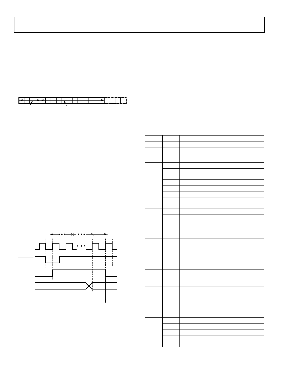
Timing
Figure 31 gives details of the ADC timing. The user controls the
ADC clock speed and the number of acquisition clocks in the
ADCCON MMR. By default, the acquisition time is eight
clocks, and the clock divider is two. The number of extra clocks
(such as bit trial or write) is set to 19, which gives a sampling
rate of 774 kSPS. For conversion on temperature sensor, the
ADC acquisition time is automatically set to 16 clocks, and the
ADC clock divider is set to 32. When using multiple channels
including the temperature sensor, the timing settings revert to
the user-defined settings after reading the temperature sensor
channel.
0
912
3-
015
ADC CLOCK
ACQ
BIT TRIAL
DATA
ADCSTA = 0
ADCSTA = 1
ADC INTERRUPT
WRITE
CONVSTART
ADCBUSY
ADCDAT
Figure 31. ADC Timing
MMRS INTERFACE
The ADC is controlled and configured via the eight MMRs.
ADCCON Register
Name:
ADCCON
Address:
0xFFFF0500
Default Value:
0x0600
Access:
Read/write
ADCCON is an ADC control register that allows the program-
mer to enable the ADC peripheral, select the mode of operation
of the ADC (either in single-ended mode, pseudo differential
mode, or fully differential mode), and select the conversion
type. This MMR is described in Table 30.
Table 30. ADCCON MMR Bit Descriptions
Bit
Value
Description
[15:14]
Reserved.
13
Set by the user to enable edge trigger mode.
Cleared by the user to enable level trigger
mode.
[12:10]
ADC clock speed.
000
fADC/1. This divider is provided to obtain
1 MSPS ADC with an external clock <41.78 MHz.
001
fADC/2 (default value).
010
fADC/4.
011
fADC/8.
100
fADC/16.
101
fADC/32.
[9:8]
ADC acquisition time.
00
Two clocks.
01
Four clocks.
10
Eight clocks (default value).
11
16 clocks.
7
Enable start conversion.
Set by the user to start any type of
conversion command.
Cleared by the user to disable a start
conversion (clearing this bit does not stop
the ADC when continuously converting).
6
Enable ADCBUSY.
Set by the user to enable the ADCBUSY pin.
Cleared by the user to disable the ADCBUSY pin.
5
ADC power control.
Set by the user to place the ADC in normal
mode (the ADC must be powered up for at least
5 μs before it converts correctly).
Cleared by the user to place the ADC in power-
down mode.
[4:3]
Conversion mode.
00
Single-ended mode.
01
Differential mode.
10
Pseudo differential mode.
11
Reserved.
相关PDF资料 |
PDF描述 |
|---|---|
| ECM30DCWN | CONN EDGECARD 60POS DIP .156 SLD |
| EVAL-ADUC7121QSPZ | BOARD EVALUATION FOR ADUC7121 |
| EVAL-ADUC7126QSPZ | BOARD EVALUATION FOR ADUC7126 |
| REC5-243.3SRWZ/H4/A | CONV DC/DC 5W 9-36VIN 3.3VOUT |
| EVAL-ADUC7023QSPZ | KIT DEV FOR ADUC7023 QUICK START |
相关代理商/技术参数 |
参数描述 |
|---|---|
| EVAL-ADUC7126QSPZ | 功能描述:BOARD EVALUATION FOR ADUC7126 RoHS:是 类别:编程器,开发系统 >> 通用嵌入式开发板和套件(MCU、DSP、FPGA、CPLD等) 系列:MicroConverter® ADuC7xxx 标准包装:1 系列:PICDEM™ 类型:MCU 适用于相关产品:PIC10F206,PIC16F690,PIC16F819 所含物品:板,线缆,元件,CD,PICkit 编程器 产品目录页面:659 (CN2011-ZH PDF) |
| EVAL-ADUC7128QSPZ | 功能描述:KIT DEV FOR ADUC7128 RoHS:是 类别:编程器,开发系统 >> 通用嵌入式开发板和套件(MCU、DSP、FPGA、CPLD等) 系列:QuickStart™ PLUS 套件 产品培训模块:Blackfin® Processor Core Architecture Overview Blackfin® Device Drivers Blackfin® Optimizations for Performance and Power Consumption Blackfin® System Services 特色产品:Blackfin? BF50x Series Processors 标准包装:1 系列:Blackfin® 类型:DSP 适用于相关产品:ADSP-BF548 所含物品:板,软件,4x4 键盘,光学拨轮,QVGA 触摸屏 LCD 和 40G 硬盘 配用:ADZS-BFBLUET-EZEXT-ND - EZ-EXTENDER DAUGHTERBOARDADZS-BFLLCD-EZEXT-ND - BOARD EXT LANDSCAP LCD INTERFACE 相关产品:ADSP-BF542BBCZ-4A-ND - IC DSP 16BIT 400MHZ 400CSBGAADSP-BF544MBBCZ-5M-ND - IC DSP 16BIT 533MHZ MDDR 400CBGAADSP-BF542MBBCZ-5M-ND - IC DSP 16BIT 533MHZ MDDR 400CBGAADSP-BF542KBCZ-6A-ND - IC DSP 16BIT 600MHZ 400CSBGAADSP-BF547MBBCZ-5M-ND - IC DSP 16BIT 533MHZ MDDR 400CBGAADSP-BF548BBCZ-5A-ND - IC DSP 16BIT 533MHZ 400CSBGAADSP-BF547BBCZ-5A-ND - IC DSP 16BIT 533MHZ 400CSBGAADSP-BF544BBCZ-5A-ND - IC DSP 16BIT 533MHZ 400CSBGAADSP-BF542BBCZ-5A-ND - IC DSP 16BIT 533MHZ 400CSBGA |
| EVAL-ADUC7128QSPZ2 | 制造商:AD 制造商全称:Analog Devices 功能描述:Precision Analog Microcontroller ARM7TDMI MCU with 12-Bit ADC and DDS DAC |
| EVAL-ADUC7129QSPZ | 制造商:Analog Devices 功能描述:- Bulk |
| EVAL-ADUC812QS | 制造商:Analog Devices 功能描述:DEVELOPMENT KIT SYSTEM |
发布紧急采购,3分钟左右您将得到回复。