- 您现在的位置:买卖IC网 > PDF目录17109 > EVAL-ADUC7122QSPZ (Analog Devices Inc)BOARD EVALUATION FOR ADUC7122 PDF资料下载
参数资料
| 型号: | EVAL-ADUC7122QSPZ |
| 厂商: | Analog Devices Inc |
| 文件页数: | 15/96页 |
| 文件大小: | 0K |
| 描述: | BOARD EVALUATION FOR ADUC7122 |
| 设计资源: | EVAL-ADUC7122 Schematic ADUC7122 Gerber Files ADUC7122 BOM |
| 标准包装: | 1 |
| 系列: | MicroConverter® ADuC7xxx |
| 类型: | MCU |
| 适用于相关产品: | ADUC7122 |
| 所含物品: | 板 |
第1页第2页第3页第4页第5页第6页第7页第8页第9页第10页第11页第12页第13页第14页当前第15页第16页第17页第18页第19页第20页第21页第22页第23页第24页第25页第26页第27页第28页第29页第30页第31页第32页第33页第34页第35页第36页第37页第38页第39页第40页第41页第42页第43页第44页第45页第46页第47页第48页第49页第50页第51页第52页第53页第54页第55页第56页第57页第58页第59页第60页第61页第62页第63页第64页第65页第66页第67页第68页第69页第70页第71页第72页第73页第74页第75页第76页第77页第78页第79页第80页第81页第82页第83页第84页第85页第86页第87页第88页第89页第90页第91页第92页第93页第94页第95页第96页
ADuC7122
Rev. 0 | Page 22 of 96
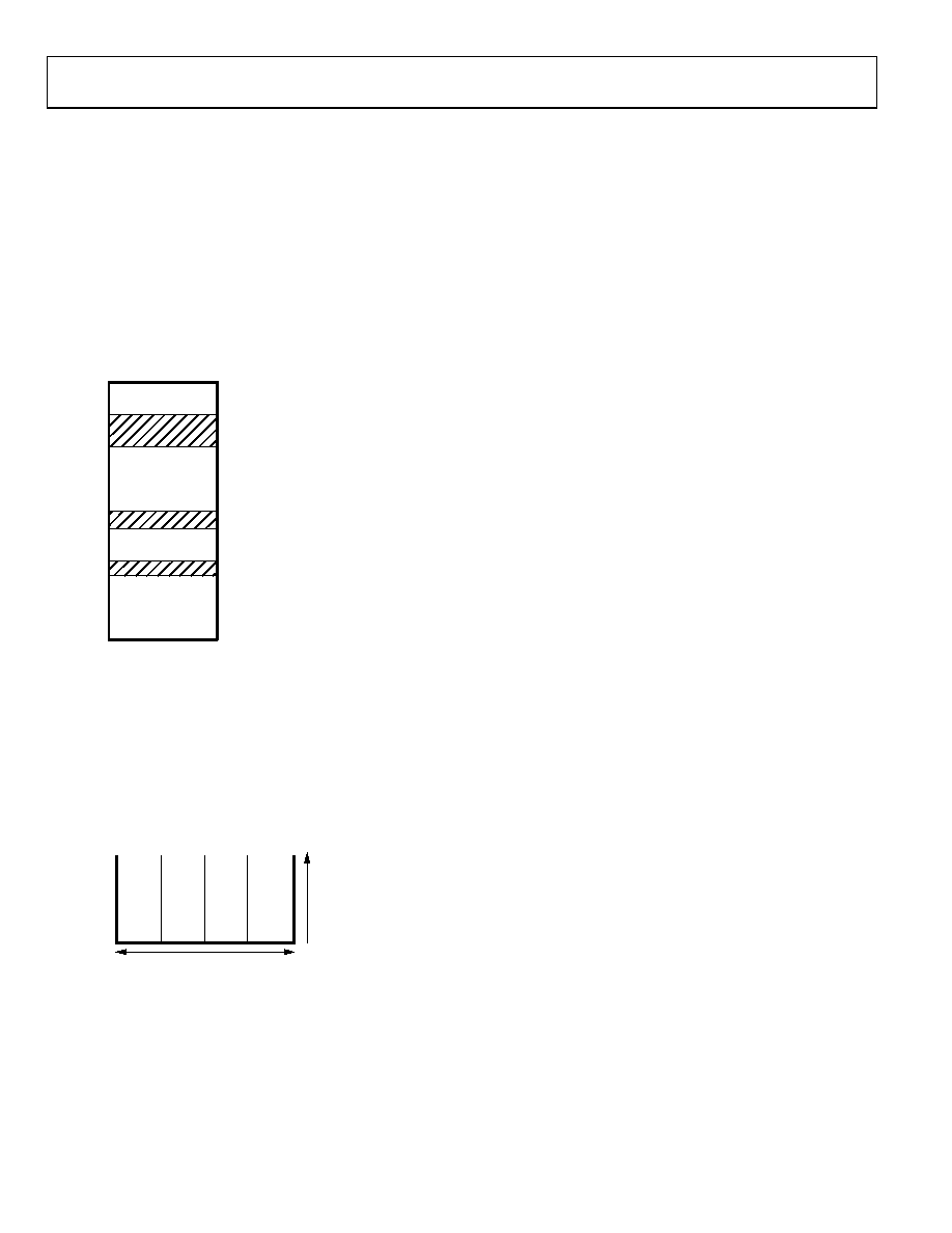
MEMORY ORGANIZATION
The ADuC7122 incorporates three separate blocks of memory:
8 kB of SRAM and two 64 kB of on-chip Flash/EE memory.
There are 126 kB of on-chip Flash/EE memory available to the
user, and the remaining 2 kB are reserved for the factory-
configured boot page. These two blocks are mapped as shown
Note that by default, after a reset, the Flash/EE memory is
mirrored at Address 0x00000000. It is possible to remap the
SRAM at Address 0x00000000 by clearing Bit 0 of the REMAP
MMR. This remap function is described in more detail in the
Flash/EE Memory section.
RESERVED
0x00080000
FLASH/EE
RESERVED
0x00041FFF
0x00040000
SRAM
0xFFFF0000
0xFFFFFFFF
MMRs
0x0001FFFF
0x00000000
0x0009F800
RESERVED
REMAPPABLE MEMORY SPACE
(FLASH/EE OR SRAM)
08
75
5-
00
9
Figure 9. Physical Memory Map
Memory Access
The ARM7 core sees memory as a linear array of 232 byte loca-
tions, where the different blocks of memory are mapped as
outlined in Figure 9.
The ADuC7122 memory organization is configured in little
endian format: the least significant byte is located in the lowest
byte address and the most significant byte in the highest byte
address.
BIT 31
BYTE 2
A
6
2
.
BYTE 3
B
7
3
.
BYTE 1
9
5
1
.
BYTE 0
8
4
0
.
BIT 0
32 BITS
0xFFFFFFFF
0x00000004
0x00000000
08
75
5-
01
0
Figure 10. Little Endian Format
FLASH/EE MEMORY
The 128 kB of Flash/EE are organized as two banks of 32k ×
16 bits. In the upper memory block, 31k × 16 bits are user
space, and 1k × 16 bits are reserved for the factory-configured
boot page. The page size of this Flash/EE memory is 512 bytes.
The lower 64 kB memory block is organized in a similar
manner. It is arranged in 32k × 16 bits. All of this is available as
user space.
The 126 kB of Flash/EE are available to the user as code and
nonvolatile data memory. There is no distinction between data
and program because ARM code shares the same space. The real
width of the Flash/EE memory is 16 bits, meaning that in ARM
mode (32-bit instruction), two accesses to the Flash/EE are
necessary for each instruction fetch. Therefore, it is
recommended that Thumb mode be used when executing from
Flash/EE memory for optimum access speed. The maximum
access speed for the Flash/EE memory is 41.78 MHz in Thumb
mode and 20.89 MHz in full ARM mode (see the Execution
Time from SRAM and FLASH/EE section).
SRAM
The 8 kB of SRAM are available to the user, organized as 2k ×
32 bits, that is, 2k words. ARM code can run directly from SRAM
at 41.78 MHz, given that the SRAM array is configured as a
32-bit wide memory array (see the Execution Time from SRAM
and FLASH/EE section).
MEMORY MAPPED REGISTERS
The memory mapped register (MMR) space is mapped into the
upper two pages of the memory array and accessed by indirect
addressing through the ARM7 banked registers.
The MMR space provides an interface between the CPU and all
on-chip peripherals. All registers except the core registers reside
in the MMR area. All shaded locations shown in Figure 11 are
unoccupied or reserved locations and should not be accessed by
user software. Table 10 to Table 26 show a full MMR memory map.
The access time reading or writing a MMR depends on the
advanced microcontroller bus architecture (AMBA) bus used to
access the peripheral. The processor has two AMBA buses:
advanced high performance bus (AHB) used for system
modules and advanced peripheral bus (APB) used for lower
performance peripheral. Access to the AHB is one cycle, and
access to the APB is two cycles. All peripherals on the
ADuC7122 are on the APB except the Flash/EE memory and
the GPIOs.
相关PDF资料 |
PDF描述 |
|---|---|
| EVAL-ADUC7124QSPZ | BOARD EVALUATION FOR ADUC7124 |
| ECM30DCWN | CONN EDGECARD 60POS DIP .156 SLD |
| EVAL-ADUC7121QSPZ | BOARD EVALUATION FOR ADUC7121 |
| EVAL-ADUC7126QSPZ | BOARD EVALUATION FOR ADUC7126 |
| REC5-243.3SRWZ/H4/A | CONV DC/DC 5W 9-36VIN 3.3VOUT |
相关代理商/技术参数 |
参数描述 |
|---|---|
| EVAL-ADUC7124QSPZ | 功能描述:BOARD EVALUATION FOR ADUC7124 RoHS:是 类别:编程器,开发系统 >> 通用嵌入式开发板和套件(MCU、DSP、FPGA、CPLD等) 系列:MicroConverter® ADuC7xxx 标准包装:1 系列:PICDEM™ 类型:MCU 适用于相关产品:PIC10F206,PIC16F690,PIC16F819 所含物品:板,线缆,元件,CD,PICkit 编程器 产品目录页面:659 (CN2011-ZH PDF) |
| EVAL-ADUC7126QSPZ | 功能描述:BOARD EVALUATION FOR ADUC7126 RoHS:是 类别:编程器,开发系统 >> 通用嵌入式开发板和套件(MCU、DSP、FPGA、CPLD等) 系列:MicroConverter® ADuC7xxx 标准包装:1 系列:PICDEM™ 类型:MCU 适用于相关产品:PIC10F206,PIC16F690,PIC16F819 所含物品:板,线缆,元件,CD,PICkit 编程器 产品目录页面:659 (CN2011-ZH PDF) |
| EVAL-ADUC7128QSPZ | 功能描述:KIT DEV FOR ADUC7128 RoHS:是 类别:编程器,开发系统 >> 通用嵌入式开发板和套件(MCU、DSP、FPGA、CPLD等) 系列:QuickStart™ PLUS 套件 产品培训模块:Blackfin® Processor Core Architecture Overview Blackfin® Device Drivers Blackfin® Optimizations for Performance and Power Consumption Blackfin® System Services 特色产品:Blackfin? BF50x Series Processors 标准包装:1 系列:Blackfin® 类型:DSP 适用于相关产品:ADSP-BF548 所含物品:板,软件,4x4 键盘,光学拨轮,QVGA 触摸屏 LCD 和 40G 硬盘 配用:ADZS-BFBLUET-EZEXT-ND - EZ-EXTENDER DAUGHTERBOARDADZS-BFLLCD-EZEXT-ND - BOARD EXT LANDSCAP LCD INTERFACE 相关产品:ADSP-BF542BBCZ-4A-ND - IC DSP 16BIT 400MHZ 400CSBGAADSP-BF544MBBCZ-5M-ND - IC DSP 16BIT 533MHZ MDDR 400CBGAADSP-BF542MBBCZ-5M-ND - IC DSP 16BIT 533MHZ MDDR 400CBGAADSP-BF542KBCZ-6A-ND - IC DSP 16BIT 600MHZ 400CSBGAADSP-BF547MBBCZ-5M-ND - IC DSP 16BIT 533MHZ MDDR 400CBGAADSP-BF548BBCZ-5A-ND - IC DSP 16BIT 533MHZ 400CSBGAADSP-BF547BBCZ-5A-ND - IC DSP 16BIT 533MHZ 400CSBGAADSP-BF544BBCZ-5A-ND - IC DSP 16BIT 533MHZ 400CSBGAADSP-BF542BBCZ-5A-ND - IC DSP 16BIT 533MHZ 400CSBGA |
| EVAL-ADUC7128QSPZ2 | 制造商:AD 制造商全称:Analog Devices 功能描述:Precision Analog Microcontroller ARM7TDMI MCU with 12-Bit ADC and DDS DAC |
| EVAL-ADUC7129QSPZ | 制造商:Analog Devices 功能描述:- Bulk |
发布紧急采购,3分钟左右您将得到回复。