- 您现在的位置:买卖IC网 > PDF目录17109 > EVAL-ADUC7023QSPZ (Analog Devices Inc)KIT DEV FOR ADUC7023 QUICK START PDF资料下载
参数资料
| 型号: | EVAL-ADUC7023QSPZ |
| 厂商: | Analog Devices Inc |
| 文件页数: | 8/96页 |
| 文件大小: | 0K |
| 描述: | KIT DEV FOR ADUC7023 QUICK START |
| 标准包装: | 1 |
| 类型: | MCU |
| 适用于相关产品: | ARM7TDMI |
| 所含物品: | 板 |
第1页第2页第3页第4页第5页第6页第7页当前第8页第9页第10页第11页第12页第13页第14页第15页第16页第17页第18页第19页第20页第21页第22页第23页第24页第25页第26页第27页第28页第29页第30页第31页第32页第33页第34页第35页第36页第37页第38页第39页第40页第41页第42页第43页第44页第45页第46页第47页第48页第49页第50页第51页第52页第53页第54页第55页第56页第57页第58页第59页第60页第61页第62页第63页第64页第65页第66页第67页第68页第69页第70页第71页第72页第73页第74页第75页第76页第77页第78页第79页第80页第81页第82页第83页第84页第85页第86页第87页第88页第89页第90页第91页第92页第93页第94页第95页第96页
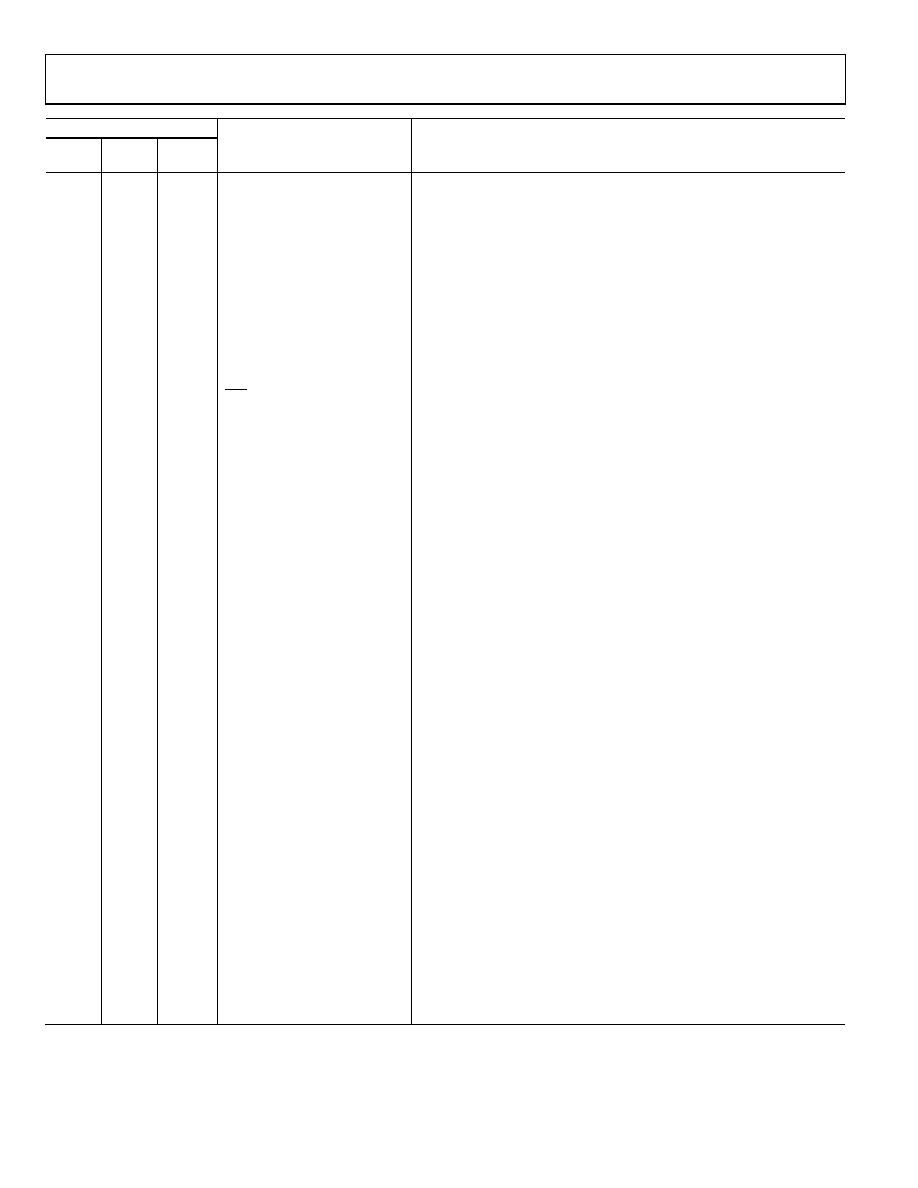
ADuC7023
Data Sheet
| Page 16 of 96
Pin No.
40-
LFCSP
32-
LFCSP
36-
WLCSP
Mnemonic
Description
28
24
C3
P0.3/PLAO[9]/TCK
The default value of this pin depends on the level of P0.0/BM. If P0.0/BM =
0, this pin defaults to a general purpose input. If P0.0/BM = 1, this pin
defaults to a JTAG test data clock pin. This is a multifunction pin as follows:
General-Purpose Input and Output Port 0.3.
Programmable Logic Array Output Element 9.
Test Clock, JTAG Test Port Clock Input. Debug and download access. When
debugging the part via JTAG, this pin must not be toggled by user code
and the GP0CON/GP0DAT register bits affecting this pin must not be
changed.
17
13
E3
DGND
Digital Ground.
18
14
F3
IOVDD
3.3 V Supply for GPIO and Input of the On-Chip Voltage Regulator.
19
15
D3
LVDD
2.6 V Output of the On-Chip Voltage Regulator. This output must be
connected to a 0.47 F capacitor to DGND only.
20
16
F2
RST
Reset Input, Active Low.
23
19
E1
RTCK
Return JTAG Clock Signal. This is not the standard JTAG clock signal. It is
an output signal from the JTAG controller. If using a 20-lead JTAG header,
connect to Pin 11.
9
7
F6
P0.4/IRQ0/SCL0/PLAI[0]/CONV
General-Purpose Input and Output Port 0.4/External Interrupt Request 0/ I2C0
Clock Signal/Programmable Logic Array Input Element 0/ADC External
Convert Start. By default, this pin is configured as a digital input with a
weak pull-up resistor enabled.
10
8
E5
P0.5/SDA0/PLAI[1]/COMPOUT
General-Purpose Input and Output Port 0.5/I2C0 Data Signal/ Programmable
Logic Array Input Element 1/Voltage Comparator Output. By default, this
pin is configured as a digital input with a weak pull-up resistor enabled.
11
9
F5
P0.6/MISO/SCL1/PLAI[2]
General-Purpose Input and Output Port 0.6/SPI MISO Signal/I2C1 Clock On
32-Lead and 36-Ball Packages/Programmable Logic Array Input Element 2.
By default, this pin is configured as a digital input with a weak pull-up
resistor enabled.
12
10
D4
P0.7/MOSI/SDA1/PLAO[0]
General-Purpose Input and Output Port 0.7/SPI MOSI Signal/I2C1 Data
Signal On 32-Lead and 36-Ball Packages/Programmable Logic Array Output
Element 0.
By default, this pin is configured as a digital input with a weak pull-up
resistor enabled.
21
17
F1
XCLKI
Input to the Crystal Oscillator Inverter and Input to the Internal Clock
Generator Circuits. Connect to DGND if unused.
22
18
E2
XCLKO
Output from the Crystal Oscillator Inverter. Leave unconnected if unused.
16
N/A
P1.7/PWM3/SDA1/PLAI[6]
General-Purpose Input and Output Port 1.7/PWM Output 3/I2C1 Data
Signal/Programmable Logic Array Input Element 6. By default, this pin is
configured as a digital input with a weak pull-up resistor enabled.
15
N/A
P1.6/PWM2/SCL1/PLAI[5]
General-Purpose Input and Output Port 1.6/PWM Output 2/I2C1 Clock
Signal/Programmable Logic Array Input Element 5. By default, this pin is
configured as a digital input with a weak pull-up resistor enabled.
29
N/A
P1.5/ADC6/PWMTRIPINPUT/PLAO[4]
General-Purpose Input and Output Port 1.5/ADC Single-Ended or
Differential Analog Input 6/PWMTRIPINPUT/Programmable Logic Array Output
Element 4. By default, this pin is configured as a digital input with a weak
pull-up resistor enabled. When used as ADC input, the pull-up resistor
should be disabled manually.
7
N/A
P1.4/ADC10/PLAO[3]
General-Purpose Input and Output Port 1.4/ADC Single-Ended or Dif-
ferential Analog Input 10/Programmable Logic Array Output Element 3.
By default, this pin is configured as a digital input with a weak pull-up
resistor enabled. When used as ADC input, the pull-up resistor should be
disabled manually.
Rev. E
相关PDF资料 |
PDF描述 |
|---|---|
| RPS-1K-6-250/2.0-9 | HEAT SHRINK SLEEVE |
| ECM30DCWH | CONN EDGECARD 60POS DIP .156 SLD |
| SC43B-3R3 | INDUCTOR SMD 3.3UH 1.44A 7.96MHZ |
| EVAL-ADUC842QSPZ | KIT DEV QUICK START ADUC842 |
| EVAL-ADUC841QSPZ | KIT DEV QUICK START ADUC841 |
相关代理商/技术参数 |
参数描述 |
|---|---|
| EVAL-ADUC7023QSPZ1 | 功能描述:BOARD EVAL FOR ADUC7023 RoHS:是 类别:编程器,开发系统 >> 通用嵌入式开发板和套件(MCU、DSP、FPGA、CPLD等) 系列:QuickStart™ PLUS 套件 产品培训模块:Blackfin® Processor Core Architecture Overview Blackfin® Device Drivers Blackfin® Optimizations for Performance and Power Consumption Blackfin® System Services 特色产品:Blackfin? BF50x Series Processors 标准包装:1 系列:Blackfin® 类型:DSP 适用于相关产品:ADSP-BF548 所含物品:板,软件,4x4 键盘,光学拨轮,QVGA 触摸屏 LCD 和 40G 硬盘 配用:ADZS-BFBLUET-EZEXT-ND - EZ-EXTENDER DAUGHTERBOARDADZS-BFLLCD-EZEXT-ND - BOARD EXT LANDSCAP LCD INTERFACE 相关产品:ADSP-BF542BBCZ-4A-ND - IC DSP 16BIT 400MHZ 400CSBGAADSP-BF544MBBCZ-5M-ND - IC DSP 16BIT 533MHZ MDDR 400CBGAADSP-BF542MBBCZ-5M-ND - IC DSP 16BIT 533MHZ MDDR 400CBGAADSP-BF542KBCZ-6A-ND - IC DSP 16BIT 600MHZ 400CSBGAADSP-BF547MBBCZ-5M-ND - IC DSP 16BIT 533MHZ MDDR 400CBGAADSP-BF548BBCZ-5A-ND - IC DSP 16BIT 533MHZ 400CSBGAADSP-BF547BBCZ-5A-ND - IC DSP 16BIT 533MHZ 400CSBGAADSP-BF544BBCZ-5A-ND - IC DSP 16BIT 533MHZ 400CSBGAADSP-BF542BBCZ-5A-ND - IC DSP 16BIT 533MHZ 400CSBGA |
| EVAL-ADuC7023QSPZ2 | 制造商:AD 制造商全称:Analog Devices 功能描述:Precision Analog Microcontroller, 12-Bit Analog I/O, ARM7TDMI MCU with Enhanced IRQ Handler |
| EVALADUC7023QSPZU1 | 制造商:Analog Devices 功能描述: |
| EVAL-ADUC7024QS | 制造商:Analog Devices 功能描述:QUICK START DEVELOPMENT SYSTEM - Bulk |
| EVAL-ADUC7024QS-U2 | 制造商:Analog Devices 功能描述:QUICK START DEVL SYST EVAL BOARD I.C. - Bulk |
发布紧急采购,3分钟左右您将得到回复。