- 您现在的位置:买卖IC网 > PDF目录17109 > EVAL-ADUC7023QSPZ (Analog Devices Inc)KIT DEV FOR ADUC7023 QUICK START PDF资料下载
参数资料
| 型号: | EVAL-ADUC7023QSPZ |
| 厂商: | Analog Devices Inc |
| 文件页数: | 22/96页 |
| 文件大小: | 0K |
| 描述: | KIT DEV FOR ADUC7023 QUICK START |
| 标准包装: | 1 |
| 类型: | MCU |
| 适用于相关产品: | ARM7TDMI |
| 所含物品: | 板 |
第1页第2页第3页第4页第5页第6页第7页第8页第9页第10页第11页第12页第13页第14页第15页第16页第17页第18页第19页第20页第21页当前第22页第23页第24页第25页第26页第27页第28页第29页第30页第31页第32页第33页第34页第35页第36页第37页第38页第39页第40页第41页第42页第43页第44页第45页第46页第47页第48页第49页第50页第51页第52页第53页第54页第55页第56页第57页第58页第59页第60页第61页第62页第63页第64页第65页第66页第67页第68页第69页第70页第71页第72页第73页第74页第75页第76页第77页第78页第79页第80页第81页第82页第83页第84页第85页第86页第87页第88页第89页第90页第91页第92页第93页第94页第95页第96页
Data Sheet
ADuC7023
| Page 29 of 96
ADC CIRCUIT OVERVIEW
The analog-to-digital converter (ADC) incorporates a fast,
multichannel, 12-bit ADC. It can operate from 2.7 V to 3.6 V
supplies and is capable of providing a throughput of up to
1 MSPS when the clock source is 41.78 MHz. This block
provides the user with a multichannel multiplexer, a differential
track-and-hold, an on-chip reference, and an ADC.
The ADC consists of a 12-bit successive approximation
converter based around two capacitor DACs. Depending on the
input signal configuration, the ADC can operate in one of two
different modes: fully differential mode (for small and balanced
signals) or single-ended mode (for any single-ended signals).
The converter accepts an analog input range of 0 V to VREF when
operating in single-ended mode. In fully differential mode, the
input signal must be balanced around a common-mode voltage
(VCM) in the 0 V to AVDD range with a maximum amplitude of
08
67
5-
0
12
AVDD
VCM
0
2VREF
Figure 19. Examples of Balanced Signals in Fully Differential Mode
A high precision, low drift, factory calibrated, 2.5 V reference is
provided on chip. An external reference can also be connected as
described later in the Band Gap Reference section.
Single or continuous conversion modes can be initiated in the
software. An external CONVSTART pin, an output generated from
the on-chip PLA, or a Timer0 or Timer1 overflow can also be
used to generate a repetitive trigger for ADC conversions.
A voltage output from an on-chip band gap reference propor-
tional to absolute temperature can also be routed through the
front-end ADC multiplexer. This temperature channel can be
selected as an ADC input. This facilitates an internal temperature
sensor channel that measures die temperature.
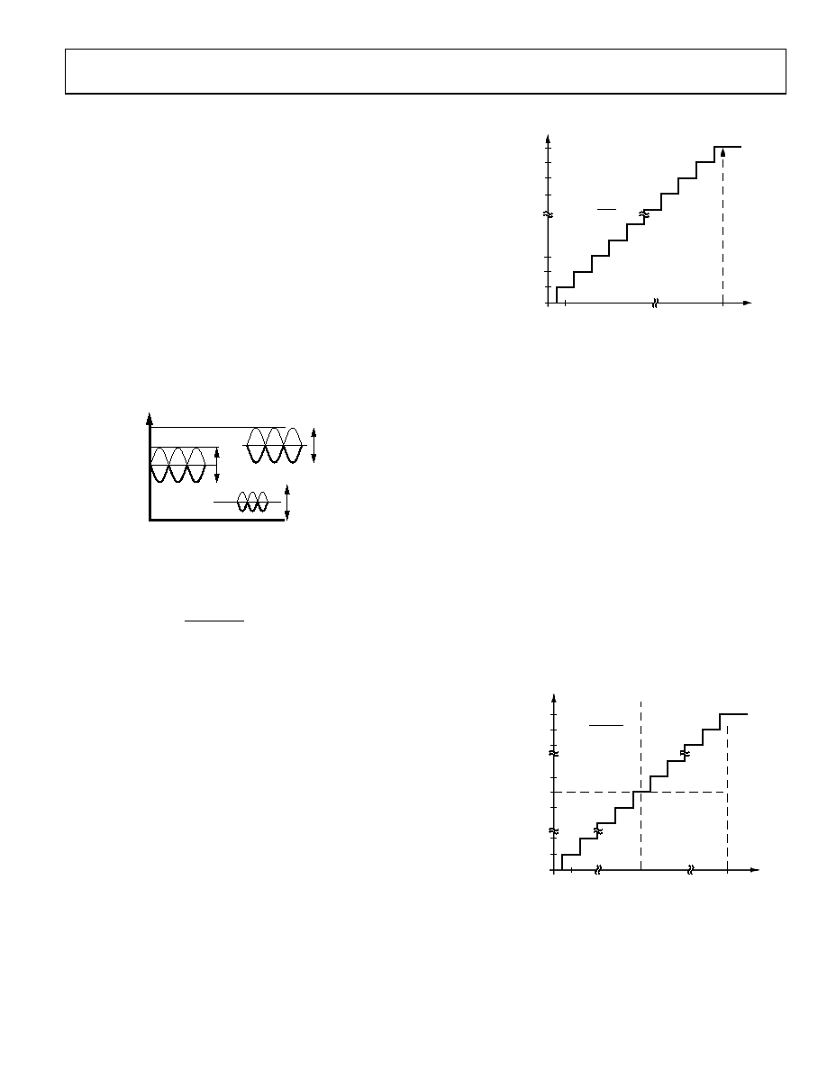
TRANSFER FUNCTION
Single-Ended Mode
In single-ended mode, the input range is 0 V to VREF. The
output coding is straight binary in single-ended mode with
1 LSB = FS/4096, or
2.5 V/4096 = 0.61 mV, or
610 μV when VREF = 2.5 V
The ideal code transitions occur midway between successive
integer LSB values (that is, 1/2 LSB, 3/2 LSB, 5/2 LSB, … ,
FS 3/2 LSB). The ideal input/output transfer characteristic
is shown in Figure 20.
086
75-
0
13
O
UT
P
UT
CO
DE
VOLTAGE INPUT
1111 1111 1111
1111 1111 1110
1111 1111 1101
1111 1111 1100
0000 0000 0011
1LSB
0V
+FS – 1LSB
0000 0000 0010
0000 0000 0001
0000 0000 0000
1LSB =
FS
4096
Figure 20. ADC Transfer Function in Single-Ended Mode
Fully Differential Mode
The amplitude of the differential signal is the difference between
the signals applied to the VIN+ and VIN– pins (that is, VIN+
VIN). The maximum amplitude of the differential signal is,
therefore, VREF to +VREF p-p (that is, 2 × VREF). This is regardless of
the common mode (CM). The common mode is the average of
the two signals, for example, (VIN+ + VIN–)/2, and is, therefore,
the voltage on which the two inputs are centered. This results in
the span of each input being CM ±VREF/2. This voltage has to be
the Analog Inputs section).
The output coding is twos complement in fully differential mode
with 1 LSB = 2 VREF/4096 or 2 × 2.5 V/4096 = 1.22 mV when
VREF = 2.5 V. The output result is ±11 bits, but this is shifted by
one to the right. This allows the result in the ADCDAT MMR to
be declared as a signed integer when writing C code. The
designed code transitions occur midway between successive
integer LSB values (that is, 1/2 LSB, 3/2 LSB, 5/2 LSB, … , FS
3/2 LSB). The ideal input/output transfer characteristic is shown
086
75
-014
O
UT
P
UT
CO
DE
VOLTAGE INPUT (VIN+ – VIN–)
0 1111 1111 1110
0 1111 1111 1100
0 1111 1111 1010
0 0000 0000 0010
0 0000 0000 0000
1 1111 1111 1110
1 0000 0000 0100
1 0000 0000 0010
1 0000 0000 0000
–VREF + 1LSB
+VREF – 1LSB
0LSB
1LSB =
2 × VREF
4096
SIGN
BIT
Figure 21. ADC Transfer Function in Differential Mode
Rev. E
相关PDF资料 |
PDF描述 |
|---|---|
| RPS-1K-6-250/2.0-9 | HEAT SHRINK SLEEVE |
| ECM30DCWH | CONN EDGECARD 60POS DIP .156 SLD |
| SC43B-3R3 | INDUCTOR SMD 3.3UH 1.44A 7.96MHZ |
| EVAL-ADUC842QSPZ | KIT DEV QUICK START ADUC842 |
| EVAL-ADUC841QSPZ | KIT DEV QUICK START ADUC841 |
相关代理商/技术参数 |
参数描述 |
|---|---|
| EVAL-ADUC7023QSPZ1 | 功能描述:BOARD EVAL FOR ADUC7023 RoHS:是 类别:编程器,开发系统 >> 通用嵌入式开发板和套件(MCU、DSP、FPGA、CPLD等) 系列:QuickStart™ PLUS 套件 产品培训模块:Blackfin® Processor Core Architecture Overview Blackfin® Device Drivers Blackfin® Optimizations for Performance and Power Consumption Blackfin® System Services 特色产品:Blackfin? BF50x Series Processors 标准包装:1 系列:Blackfin® 类型:DSP 适用于相关产品:ADSP-BF548 所含物品:板,软件,4x4 键盘,光学拨轮,QVGA 触摸屏 LCD 和 40G 硬盘 配用:ADZS-BFBLUET-EZEXT-ND - EZ-EXTENDER DAUGHTERBOARDADZS-BFLLCD-EZEXT-ND - BOARD EXT LANDSCAP LCD INTERFACE 相关产品:ADSP-BF542BBCZ-4A-ND - IC DSP 16BIT 400MHZ 400CSBGAADSP-BF544MBBCZ-5M-ND - IC DSP 16BIT 533MHZ MDDR 400CBGAADSP-BF542MBBCZ-5M-ND - IC DSP 16BIT 533MHZ MDDR 400CBGAADSP-BF542KBCZ-6A-ND - IC DSP 16BIT 600MHZ 400CSBGAADSP-BF547MBBCZ-5M-ND - IC DSP 16BIT 533MHZ MDDR 400CBGAADSP-BF548BBCZ-5A-ND - IC DSP 16BIT 533MHZ 400CSBGAADSP-BF547BBCZ-5A-ND - IC DSP 16BIT 533MHZ 400CSBGAADSP-BF544BBCZ-5A-ND - IC DSP 16BIT 533MHZ 400CSBGAADSP-BF542BBCZ-5A-ND - IC DSP 16BIT 533MHZ 400CSBGA |
| EVAL-ADuC7023QSPZ2 | 制造商:AD 制造商全称:Analog Devices 功能描述:Precision Analog Microcontroller, 12-Bit Analog I/O, ARM7TDMI MCU with Enhanced IRQ Handler |
| EVALADUC7023QSPZU1 | 制造商:Analog Devices 功能描述: |
| EVAL-ADUC7024QS | 制造商:Analog Devices 功能描述:QUICK START DEVELOPMENT SYSTEM - Bulk |
| EVAL-ADUC7024QS-U2 | 制造商:Analog Devices 功能描述:QUICK START DEVL SYST EVAL BOARD I.C. - Bulk |
发布紧急采购,3分钟左右您将得到回复。