- 您现在的位置:买卖IC网 > PDF目录17109 > EVAL-ADUC7023QSPZ (Analog Devices Inc)KIT DEV FOR ADUC7023 QUICK START PDF资料下载
参数资料
| 型号: | EVAL-ADUC7023QSPZ |
| 厂商: | Analog Devices Inc |
| 文件页数: | 28/96页 |
| 文件大小: | 0K |
| 描述: | KIT DEV FOR ADUC7023 QUICK START |
| 标准包装: | 1 |
| 类型: | MCU |
| 适用于相关产品: | ARM7TDMI |
| 所含物品: | 板 |
第1页第2页第3页第4页第5页第6页第7页第8页第9页第10页第11页第12页第13页第14页第15页第16页第17页第18页第19页第20页第21页第22页第23页第24页第25页第26页第27页当前第28页第29页第30页第31页第32页第33页第34页第35页第36页第37页第38页第39页第40页第41页第42页第43页第44页第45页第46页第47页第48页第49页第50页第51页第52页第53页第54页第55页第56页第57页第58页第59页第60页第61页第62页第63页第64页第65页第66页第67页第68页第69页第70页第71页第72页第73页第74页第75页第76页第77页第78页第79页第80页第81页第82页第83页第84页第85页第86页第87页第88页第89页第90页第91页第92页第93页第94页第95页第96页
ADuC7023
Data Sheet
| Page 34 of 96
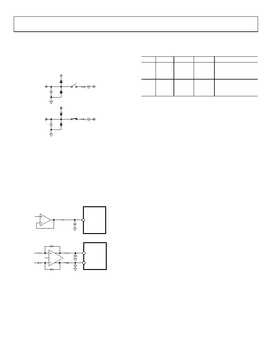
The C1 capacitors in Figure 27 are typically 4 pF and can be
primarily attributed to pin capacitance. The resistors are
lumped components made up of the on resistance of the
switches. The value of these resistors is typically about 100 .
The C2 capacitors are the ADC sampling capacitors and
typically have a capacitance of 16 pF.
AVDD
C1
D
R1 C2
AVDD
C1
D
R1 C2
08675-
021
Figure 27. Equivalent Analog Input Circuit Conversion Phase: Switches Open,
Track Phase: Switches Closed
For ac applications, removing high frequency components from
the analog input signal is recommended by using an RC low-
pass filter on the relevant analog input pins. In applications
where harmonic distortion and signal-to-noise ratio are critical,
the analog input should be driven from a low impedance
source. Large source impedances significantly affect the ac
performance of the ADC. This can necessitate the use of an
input buffer amplifier. The choice of the op amp is a function of
the particular application. Figure 28 and Figure 29 give an
example of an ADC front end.
08675-
022
ADuC7023
ADC0
10
0.01F
Figure 28. Buffering Single-Ended Differential Input
08675-
023
ADuC7023
ADC0
VREF
ADC1
Figure 29. Buffering Differential Inputs
When no amplifier is used to drive the analog input, limit the
source impedance to values lower than 1 k. The maximum
source impedance depends on the amount of total harmonic
distortion (THD) that can be tolerated. The THD increases as
the source impedance increases and the performance degrades.
DRIVING THE ANALOG INPUTS
Internal or external references can be used for the ADC. When
operating in differential mode, there are restrictions on the
common-mode input signal (VCM), which is dependent upon
the reference value and supply voltage used to ensure that the
signal remains within the supply rails. Table 27 gives some
calculated VCM minimum and VCM maximum values.
Table 27. VCM Ranges
AVDD
VREF
VCM Min
VCM Max
Signal Peak-to-Peak
3.3 V
2.5 V
1.25 V
2.05 V
2.5 V
2.048 V
1.024 V
2.276 V
2.048 V
1.25 V
0.75 V
2.55 V
1.25 V
3.0 V
2.5 V
1.25 V
1.75 V
2.5 V
2.048 V
1.024 V
1.976 V
2.048 V
1.25 V
0.75 V
2.25 V
1.25 V
CALIBRATION
By default, the factory-set values written to the ADC offset
(ADCOF) and gain coefficient registers (ADCGN) yield
optimum performance in terms of endpoint errors and linearity
for standalone operation of the part (see the Specifications
section). If system calibration is required, it is possible to
modify the default offset and gain coefficients to improve
endpoint errors, but note that any modification to the factory-
set ADCOF and ADCGN values can degrade ADC linearity
performance.
For system offset error correction, the ADC channel input stage
must be tied to AGND. A continuous software ADC conversion
loop must be implemented by modifying the value in ADCOF until
the ADC result (ADCDAT) reads Code 0 to Code 1. If the
ADCDAT value is greater than 1, ADCOF should be decremented
until ADCDAT reads Code 0 to Code 1. Offset error correction
is done digitally and has a resolution of 0.25 LSB and a range of
±3.125% of VREF.
For system gain error correction, the ADC channel input
stage must be tied to VREF. A continuous software ADC
conversion loop must be implemented to modify the value
in ADCGN until the ADCDAT reads Code 4094 to Code 4095.
If the ADCDAT value is less than 4094, ADCGN should be
incremented until ADCDAT reads Code 4094 to Code 4095.
Similar to the offset calibration, the gain calibration resolution
is 0.25 LSB with a range of ±3% of VREF.
TEMPERATURE SENSOR
The ADuC7023 provides a voltage output from an on-chip
band gap reference that is proportional to absolute temperature.
This voltage output can also be routed through the front-end
ADC multiplexer (effectively an additional ADC channel
input), facilitating an internal temperature sensor channel,
measuring die temperature.
An ADC temperature sensor conversion differs from a standard
ADC voltage. The ADC performance specifications do not
apply to the temperature sensor.
Chopping of the internal amplifier should be enabled using the
TSCON register. To enable this mode, the user must set Bit 0 of
TSCON. The user must also take two consecutive ADC readings
and average them in this mode.
Rev. E
相关PDF资料 |
PDF描述 |
|---|---|
| RPS-1K-6-250/2.0-9 | HEAT SHRINK SLEEVE |
| ECM30DCWH | CONN EDGECARD 60POS DIP .156 SLD |
| SC43B-3R3 | INDUCTOR SMD 3.3UH 1.44A 7.96MHZ |
| EVAL-ADUC842QSPZ | KIT DEV QUICK START ADUC842 |
| EVAL-ADUC841QSPZ | KIT DEV QUICK START ADUC841 |
相关代理商/技术参数 |
参数描述 |
|---|---|
| EVAL-ADUC7023QSPZ1 | 功能描述:BOARD EVAL FOR ADUC7023 RoHS:是 类别:编程器,开发系统 >> 通用嵌入式开发板和套件(MCU、DSP、FPGA、CPLD等) 系列:QuickStart™ PLUS 套件 产品培训模块:Blackfin® Processor Core Architecture Overview Blackfin® Device Drivers Blackfin® Optimizations for Performance and Power Consumption Blackfin® System Services 特色产品:Blackfin? BF50x Series Processors 标准包装:1 系列:Blackfin® 类型:DSP 适用于相关产品:ADSP-BF548 所含物品:板,软件,4x4 键盘,光学拨轮,QVGA 触摸屏 LCD 和 40G 硬盘 配用:ADZS-BFBLUET-EZEXT-ND - EZ-EXTENDER DAUGHTERBOARDADZS-BFLLCD-EZEXT-ND - BOARD EXT LANDSCAP LCD INTERFACE 相关产品:ADSP-BF542BBCZ-4A-ND - IC DSP 16BIT 400MHZ 400CSBGAADSP-BF544MBBCZ-5M-ND - IC DSP 16BIT 533MHZ MDDR 400CBGAADSP-BF542MBBCZ-5M-ND - IC DSP 16BIT 533MHZ MDDR 400CBGAADSP-BF542KBCZ-6A-ND - IC DSP 16BIT 600MHZ 400CSBGAADSP-BF547MBBCZ-5M-ND - IC DSP 16BIT 533MHZ MDDR 400CBGAADSP-BF548BBCZ-5A-ND - IC DSP 16BIT 533MHZ 400CSBGAADSP-BF547BBCZ-5A-ND - IC DSP 16BIT 533MHZ 400CSBGAADSP-BF544BBCZ-5A-ND - IC DSP 16BIT 533MHZ 400CSBGAADSP-BF542BBCZ-5A-ND - IC DSP 16BIT 533MHZ 400CSBGA |
| EVAL-ADuC7023QSPZ2 | 制造商:AD 制造商全称:Analog Devices 功能描述:Precision Analog Microcontroller, 12-Bit Analog I/O, ARM7TDMI MCU with Enhanced IRQ Handler |
| EVALADUC7023QSPZU1 | 制造商:Analog Devices 功能描述: |
| EVAL-ADUC7024QS | 制造商:Analog Devices 功能描述:QUICK START DEVELOPMENT SYSTEM - Bulk |
| EVAL-ADUC7024QS-U2 | 制造商:Analog Devices 功能描述:QUICK START DEVL SYST EVAL BOARD I.C. - Bulk |
发布紧急采购,3分钟左右您将得到回复。