- 您现在的位置:买卖IC网 > PDF目录17109 > EVAL-ADUC7126QSPZ (Analog Devices Inc)BOARD EVALUATION FOR ADUC7126 PDF资料下载
参数资料
| 型号: | EVAL-ADUC7126QSPZ |
| 厂商: | Analog Devices Inc |
| 文件页数: | 89/108页 |
| 文件大小: | 0K |
| 描述: | BOARD EVALUATION FOR ADUC7126 |
| 设计资源: | EVAL-ADUC7126 Schematic ADUC7126 Gerber Files |
| 标准包装: | 1 |
| 系列: | MicroConverter® ADuC7xxx |
| 类型: | MCU |
| 适用于相关产品: | ADUC7126 |
| 所含物品: | 板 |
第1页第2页第3页第4页第5页第6页第7页第8页第9页第10页第11页第12页第13页第14页第15页第16页第17页第18页第19页第20页第21页第22页第23页第24页第25页第26页第27页第28页第29页第30页第31页第32页第33页第34页第35页第36页第37页第38页第39页第40页第41页第42页第43页第44页第45页第46页第47页第48页第49页第50页第51页第52页第53页第54页第55页第56页第57页第58页第59页第60页第61页第62页第63页第64页第65页第66页第67页第68页第69页第70页第71页第72页第73页第74页第75页第76页第77页第78页第79页第80页第81页第82页第83页第84页第85页第86页第87页第88页当前第89页第90页第91页第92页第93页第94页第95页第96页第97页第98页第99页第100页第101页第102页第103页第104页第105页第106页第107页第108页
Data Sheet
ADuC7124/ADuC7126
Rev. C | Page 81 of 108
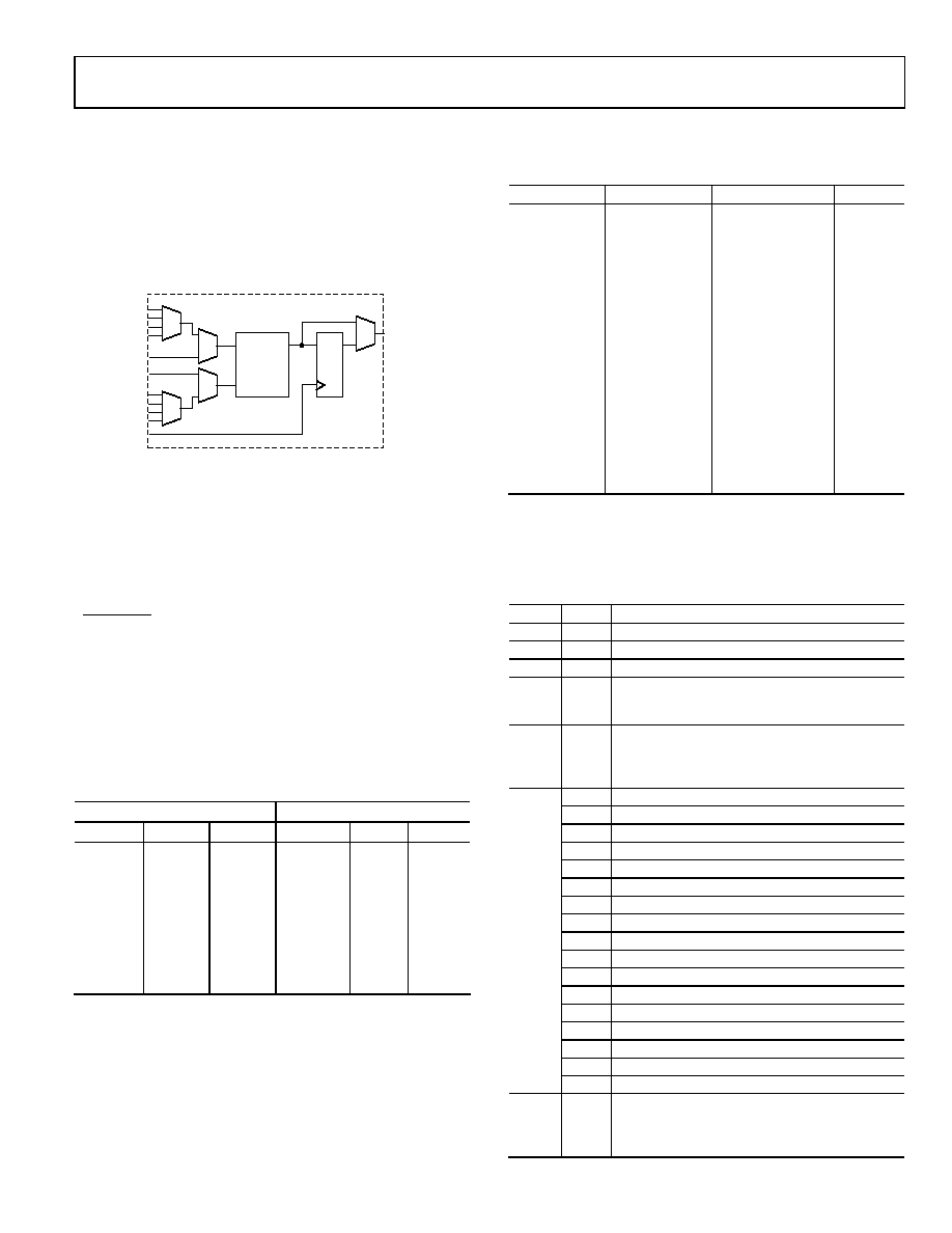
PROGRAMMABLE LOGIC ARRAY (PLA)
Every ADuC7124/ADuC7126 integrates a fully programmable
logic array (PLA) that consists of two independent but
interconnected PLA blocks. Each block consists of eight PLA
elements, giving each part a total of 16 PLA elements.
Each PLA element contains a two-input look up table that can
be configured to generate any logic output function based on
two inputs and a flip-flop. This is represented in Figure 51.
09
12
3-
1
33
4
2
0
1
3
A
B
LOOK-UP
TABLE
Figure 51. PLA Element
In total, 40 GPIO pins are available on the ADuC7124/ADuC7126
for the PLA. These include 16 input pins and 16 output pins that
must be configured in the GPxCON register as PLA pins before
using the PLA. Note that the comparator output is also included
as one of the 16 input pins.
The PLA is configured via a set of user MMRs. The output(s) of
the PLA can be routed to the internal interrupt system, to the
CONVSTART signal of the ADC, to an MMR, or to any of the 16
PLA output pins.
The two blocks can be interconnected as follows:
Output of Element 15 (Block 1) can be fed back to Input 0 of
Mux 0 of Element 0 (Block 0).
Output of Element 7 (Block 0) can be fed back to Input 0 of
Mux 0 of Element 8 (Block 1).
Table 117. Element Input/Output1
PLA Block 0
PLA Block 1
Element
Input
Output
Element
Input
Output
0
P1.0
P1.7
8
P3.0
P4.0
1
P1.1
P0.4
9
P3.1
P4.1
2
P1.2
P0.5
10
P3.2
P4.2
3
P1.3
P0.6
11
P3.3
P4.3
4
P1.4
P0.7
12
P3.4
P4.4
5
P1.5
P2.0
13
P3.5
P4.5
6
P1.6
P2.1
14
P3.6
P4.6
7
P0.0
P2.2
15
P3.7
P4.7
1 Not all pins in this table are connected to external pins. However, they may
be routed internally via the PLA. See Table 122 for further details.
PLA MMRs Interface
The PLA peripheral interface consists of the 22 MMRs.
Table 118. PLAELMx Registers
Name
Address
Default Value
Access
PLAELM0
0xFFFF0B00
0x0000
R/W
PLAELM1
0xFFFF0B04
0x0000
R/W
PLAELM2
0xFFFF0B08
0x0000
R/W
PLAELM3
0xFFFF0B0C
0x0000
R/W
PLAELM4
0xFFFF0B10
0x0000
R/W
PLAELM5
0xFFFF0B14
0x0000
R/W
PLAELM6
0xFFFF0B18
0x0000
R/W
PLAELM7
0xFFFF0B1C
0x0000
R/W
PLAELM8
0xFFFF0B20
0x0000
R/W
PLAELM9
0xFFFF0B24
0x0000
R/W
PLAELM10
0xFFFF0B28
0x0000
R/W
PLAELM11
0xFFFF0B2C
0x0000
R/W
PLAELM12
0xFFFF0B30
0x0000
R/W
PLAELM13
0xFFFF0B34
0x0000
R/W
PLAELM14
0xFFFF0B38
0x0000
R/W
PLAELM15
0xFFFF0B3C
0x0000
R/W
The PLAELMx are Element 0 to Element 15 control registers.
They configure the input and output mux of each element,
select the function in the look up table, and bypass/use the flip-
Table 119. PLAELMx MMR Bit Descriptions
Bit
Value
Description
[31:11]
Reserved.
[10:9]
Mux 0 control (see Table 122).
[8:7]
Mux 1 control (see Table 122).
6
Mux 2 control.
Set by the user to select the output of Mux 0. Cleared
by the user to select the bit value from PLADIN.
5
Mux 3 control.
Set by the user to select the input pin of the particular
element.
Cleared by the user to select the output of Mux 1.
[4:1]
Look-up table control.
0000
0.
0001
NOR.
0010
B AND NOT A.
0011
NOT A.
0100
A AND NOT B.
0101
NOT B.
0110
EXOR.
0111
NAND.
1000
AND.
1001
EXNOR.
1010
B.
1011
NOT A OR B.
1100
A.
1101
A OR NOT B.
1110
OR.
1111
1.
0
Mux 4 control.
Set by the user to bypass the flip-flop.
Cleared by the user to select the flip-flop (cleared by
default).
相关PDF资料 |
PDF描述 |
|---|---|
| REC5-243.3SRWZ/H4/A | CONV DC/DC 5W 9-36VIN 3.3VOUT |
| EVAL-ADUC7023QSPZ | KIT DEV FOR ADUC7023 QUICK START |
| RPS-1K-6-250/2.0-9 | HEAT SHRINK SLEEVE |
| ECM30DCWH | CONN EDGECARD 60POS DIP .156 SLD |
| SC43B-3R3 | INDUCTOR SMD 3.3UH 1.44A 7.96MHZ |
相关代理商/技术参数 |
参数描述 |
|---|---|
| EVAL-ADUC7128QSPZ | 功能描述:KIT DEV FOR ADUC7128 RoHS:是 类别:编程器,开发系统 >> 通用嵌入式开发板和套件(MCU、DSP、FPGA、CPLD等) 系列:QuickStart™ PLUS 套件 产品培训模块:Blackfin® Processor Core Architecture Overview Blackfin® Device Drivers Blackfin® Optimizations for Performance and Power Consumption Blackfin® System Services 特色产品:Blackfin? BF50x Series Processors 标准包装:1 系列:Blackfin® 类型:DSP 适用于相关产品:ADSP-BF548 所含物品:板,软件,4x4 键盘,光学拨轮,QVGA 触摸屏 LCD 和 40G 硬盘 配用:ADZS-BFBLUET-EZEXT-ND - EZ-EXTENDER DAUGHTERBOARDADZS-BFLLCD-EZEXT-ND - BOARD EXT LANDSCAP LCD INTERFACE 相关产品:ADSP-BF542BBCZ-4A-ND - IC DSP 16BIT 400MHZ 400CSBGAADSP-BF544MBBCZ-5M-ND - IC DSP 16BIT 533MHZ MDDR 400CBGAADSP-BF542MBBCZ-5M-ND - IC DSP 16BIT 533MHZ MDDR 400CBGAADSP-BF542KBCZ-6A-ND - IC DSP 16BIT 600MHZ 400CSBGAADSP-BF547MBBCZ-5M-ND - IC DSP 16BIT 533MHZ MDDR 400CBGAADSP-BF548BBCZ-5A-ND - IC DSP 16BIT 533MHZ 400CSBGAADSP-BF547BBCZ-5A-ND - IC DSP 16BIT 533MHZ 400CSBGAADSP-BF544BBCZ-5A-ND - IC DSP 16BIT 533MHZ 400CSBGAADSP-BF542BBCZ-5A-ND - IC DSP 16BIT 533MHZ 400CSBGA |
| EVAL-ADUC7128QSPZ2 | 制造商:AD 制造商全称:Analog Devices 功能描述:Precision Analog Microcontroller ARM7TDMI MCU with 12-Bit ADC and DDS DAC |
| EVAL-ADUC7129QSPZ | 制造商:Analog Devices 功能描述:- Bulk |
| EVAL-ADUC812QS | 制造商:Analog Devices 功能描述:DEVELOPMENT KIT SYSTEM |
| EVAL-ADUC812QSP | 制造商:AD 制造商全称:Analog Devices 功能描述:MicroConverter㈢, Multichannel 12-Bit ADC with Embedded Flash MCU |
发布紧急采购,3分钟左右您将得到回复。