- 您现在的位置:买卖IC网 > PDF目录17109 > EVAL-ADUC7126QSPZ (Analog Devices Inc)BOARD EVALUATION FOR ADUC7126 PDF资料下载
参数资料
| 型号: | EVAL-ADUC7126QSPZ |
| 厂商: | Analog Devices Inc |
| 文件页数: | 4/108页 |
| 文件大小: | 0K |
| 描述: | BOARD EVALUATION FOR ADUC7126 |
| 设计资源: | EVAL-ADUC7126 Schematic ADUC7126 Gerber Files |
| 标准包装: | 1 |
| 系列: | MicroConverter® ADuC7xxx |
| 类型: | MCU |
| 适用于相关产品: | ADUC7126 |
| 所含物品: | 板 |
第1页第2页第3页当前第4页第5页第6页第7页第8页第9页第10页第11页第12页第13页第14页第15页第16页第17页第18页第19页第20页第21页第22页第23页第24页第25页第26页第27页第28页第29页第30页第31页第32页第33页第34页第35页第36页第37页第38页第39页第40页第41页第42页第43页第44页第45页第46页第47页第48页第49页第50页第51页第52页第53页第54页第55页第56页第57页第58页第59页第60页第61页第62页第63页第64页第65页第66页第67页第68页第69页第70页第71页第72页第73页第74页第75页第76页第77页第78页第79页第80页第81页第82页第83页第84页第85页第86页第87页第88页第89页第90页第91页第92页第93页第94页第95页第96页第97页第98页第99页第100页第101页第102页第103页第104页第105页第106页第107页第108页
Data Sheet
ADuC7124/ADuC7126
Rev. C | Page 101 of 108
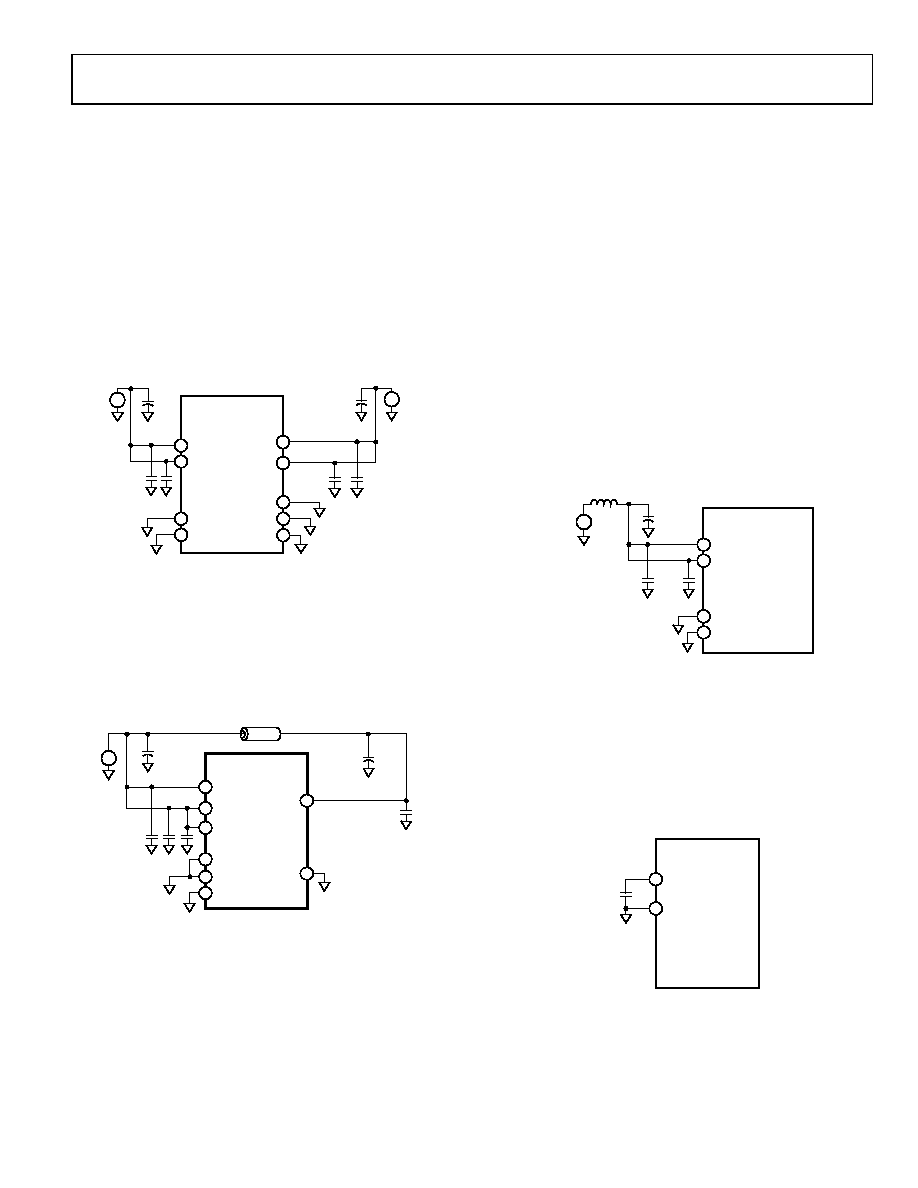
HARDWARE DESIGN CONSIDERATIONS
POWER SUPPLIES
The ADuC7124/ADuC7126 operational power supply voltage
range is 2.7 V to 3.6 V. Separate analog and digital power supply
pins (AVDD and IOVDD, respectively) allow AVDD to be kept
relatively free of noisy digital signals often present on the
system IOVDD line. In this mode, the part can also operate with
split supplies; that is, it can use different voltage levels for each
supply. For example, the system can be designed to operate
with an IOVDD voltage level of 3.3 V while the AVDD level can be
at 3 V or vice versa. A typical split supply configuration is
shown in Figure 62.
09
12
3-
0
44
ADuC7124/
ADuC7126
0.1F
ANALOG
SUPPLY
10F
AVDD
DACVDD
GNDREF
DACGND
AGND
IOVDD
IOGND
0.1F
+
–
DIGITAL
SUPPLY
10F
+
–
Figure 62. External Dual Supply Connections
As an alternative to providing two separate power supplies, the
user can reduce noise on AVDD by placing a small series resistor
and/or ferrite bead between AVDD and IOVDD and then decoupling
AVDD separately to ground. An example of this configuration is
shown in Figure 63. With this configuration, other analog circuitry
(such as op amps, voltage reference, or any other analog circuitry)
can be powered from the AVDD supply line as well.
0
91
23-
14
5
ADuC7124/
ADuC7126
0.1F
BEAD
AVDD
AGND
IOVDD
DGND
0.1F
DIGITAL SUPPLY
ANALOG SUPPLY
10F
+
–
Figure 63. External Single Supply Connections
Notice that in both Figure 62 and Figure 63, a large value (10 μF)
reservoir capacitor sits on IOVDD, and a separate 10 μF capacitor
sits on AVDD. In addition, local small-value (0.1 μF) capacitors are
located at each AVDD and IOVDD pin of the chip. As per standard
design practice, be sure to include all of these capacitors and ensure
that the smaller capacitors are close to each AVDD pin with trace
lengths as short as possible. Connect the ground terminal of
each of these capacitors directly to the underlying ground plane.
Finally, note that the analog and digital ground pins on the
ADuC7124/ADuC7126 must be referenced to the same system
ground reference point at all times.
IOVDD Supply Sensitivity
The IOVDD supply is sensitive to high frequency noise because it
is the supply source for the internal oscillator and PLL circuits.
When the internal PLL loses lock, the clock source is removed
by a gating circuit from the CPU, and the ARM7TDMI core
stops executing code until the PLL regains lock. This feature
ensures that no flash interface timings or ARM7TDMI timings
are violated.
Typically, frequency noise greater than 50 kHz and 50 mV p-p
on top of the supply causes the core to stop working.
If decoupling values recommended in the Power Supplies
section do not sufficiently dampen all noise sources below
recommended.
ADuC7124/
ADuC7126
IOVDD
IOGND
0.1F
DIGITAL
SUPPLY
10F
+
–
1H
09
12
3-
08
7
Figure 64. Recommended IOVDD Supply Filter
Linear Voltage Regulator
The ADuC7124/ADuC7126 require a single 3.3 V supply, but
the core logic requires a 2.6 V supply. An on-chip linear
regulator generates the 2.6 V from IOVDD for the core logic. The
LVDD pin is the 2.6 V supply for the core logic. An external
compensation capacitor of 0.47 μF must be connected between
LVDD and DGND (as close as possible to these pins) to act as a
tank of charge as shown in Figure 65.
0
9123
-046
ADuC7124/
ADuC7126
0.47F
LVDD
DGND
Figure 65. Voltage Regulator Connections
The LVDD pin should not be used for any other chip. It is also
recommended to use excellent power supply decoupling on
IOVDD to help improve line regulation performance of the on-
chip voltage regulator.
相关PDF资料 |
PDF描述 |
|---|---|
| REC5-243.3SRWZ/H4/A | CONV DC/DC 5W 9-36VIN 3.3VOUT |
| EVAL-ADUC7023QSPZ | KIT DEV FOR ADUC7023 QUICK START |
| RPS-1K-6-250/2.0-9 | HEAT SHRINK SLEEVE |
| ECM30DCWH | CONN EDGECARD 60POS DIP .156 SLD |
| SC43B-3R3 | INDUCTOR SMD 3.3UH 1.44A 7.96MHZ |
相关代理商/技术参数 |
参数描述 |
|---|---|
| EVAL-ADUC7128QSPZ | 功能描述:KIT DEV FOR ADUC7128 RoHS:是 类别:编程器,开发系统 >> 通用嵌入式开发板和套件(MCU、DSP、FPGA、CPLD等) 系列:QuickStart™ PLUS 套件 产品培训模块:Blackfin® Processor Core Architecture Overview Blackfin® Device Drivers Blackfin® Optimizations for Performance and Power Consumption Blackfin® System Services 特色产品:Blackfin? BF50x Series Processors 标准包装:1 系列:Blackfin® 类型:DSP 适用于相关产品:ADSP-BF548 所含物品:板,软件,4x4 键盘,光学拨轮,QVGA 触摸屏 LCD 和 40G 硬盘 配用:ADZS-BFBLUET-EZEXT-ND - EZ-EXTENDER DAUGHTERBOARDADZS-BFLLCD-EZEXT-ND - BOARD EXT LANDSCAP LCD INTERFACE 相关产品:ADSP-BF542BBCZ-4A-ND - IC DSP 16BIT 400MHZ 400CSBGAADSP-BF544MBBCZ-5M-ND - IC DSP 16BIT 533MHZ MDDR 400CBGAADSP-BF542MBBCZ-5M-ND - IC DSP 16BIT 533MHZ MDDR 400CBGAADSP-BF542KBCZ-6A-ND - IC DSP 16BIT 600MHZ 400CSBGAADSP-BF547MBBCZ-5M-ND - IC DSP 16BIT 533MHZ MDDR 400CBGAADSP-BF548BBCZ-5A-ND - IC DSP 16BIT 533MHZ 400CSBGAADSP-BF547BBCZ-5A-ND - IC DSP 16BIT 533MHZ 400CSBGAADSP-BF544BBCZ-5A-ND - IC DSP 16BIT 533MHZ 400CSBGAADSP-BF542BBCZ-5A-ND - IC DSP 16BIT 533MHZ 400CSBGA |
| EVAL-ADUC7128QSPZ2 | 制造商:AD 制造商全称:Analog Devices 功能描述:Precision Analog Microcontroller ARM7TDMI MCU with 12-Bit ADC and DDS DAC |
| EVAL-ADUC7129QSPZ | 制造商:Analog Devices 功能描述:- Bulk |
| EVAL-ADUC812QS | 制造商:Analog Devices 功能描述:DEVELOPMENT KIT SYSTEM |
| EVAL-ADUC812QSP | 制造商:AD 制造商全称:Analog Devices 功能描述:MicroConverter㈢, Multichannel 12-Bit ADC with Embedded Flash MCU |
发布紧急采购,3分钟左右您将得到回复。