- 您现在的位置:买卖IC网 > PDF目录17109 > EVAL-ADUC7126QSPZ (Analog Devices Inc)BOARD EVALUATION FOR ADUC7126 PDF资料下载
参数资料
| 型号: | EVAL-ADUC7126QSPZ |
| 厂商: | Analog Devices Inc |
| 文件页数: | 52/108页 |
| 文件大小: | 0K |
| 描述: | BOARD EVALUATION FOR ADUC7126 |
| 设计资源: | EVAL-ADUC7126 Schematic ADUC7126 Gerber Files |
| 标准包装: | 1 |
| 系列: | MicroConverter® ADuC7xxx |
| 类型: | MCU |
| 适用于相关产品: | ADUC7126 |
| 所含物品: | 板 |
第1页第2页第3页第4页第5页第6页第7页第8页第9页第10页第11页第12页第13页第14页第15页第16页第17页第18页第19页第20页第21页第22页第23页第24页第25页第26页第27页第28页第29页第30页第31页第32页第33页第34页第35页第36页第37页第38页第39页第40页第41页第42页第43页第44页第45页第46页第47页第48页第49页第50页第51页当前第52页第53页第54页第55页第56页第57页第58页第59页第60页第61页第62页第63页第64页第65页第66页第67页第68页第69页第70页第71页第72页第73页第74页第75页第76页第77页第78页第79页第80页第81页第82页第83页第84页第85页第86页第87页第88页第89页第90页第91页第92页第93页第94页第95页第96页第97页第98页第99页第100页第101页第102页第103页第104页第105页第106页第107页第108页
ADuC7124/ADuC7126
Data Sheet
Rev. C | Page 48 of 108
Table 56. FEE0PRO and FEE0HID MMR Bit Descriptions
Bit
Description
31
Read protection.
Cleared by the user to protect Block 0.
Set by the user to allow reading of Block 0.
[30:0]
Write protection for Page 123 to Page 120, for Page 119
to Page 116, and for Page 0 to Page 3.
Cleared by the user to protect the pages in writing.
Set by the user to allow writing to the pages.
Table 57. FEE1PRO and FEE1HID MMR Bit Descriptions
Bit
Description
31
Read protection.
Cleared by the user to protect Block 1.
Set by the user to allow reading of Block 1.
30
Write protection for Page 127 to Page 120.
Cleared by the user to protect the pages in writing.
Set by the user to allow writing to the pages.
[29:0]
Write protection for Page 119 to Page 116 and for Page 0
to Page 3.
Cleared by the user to protect the pages in writing.
Set by the user to allow writing to the pages.
EXECUTION TIME FROM SRAM AND FLASH/EE
This section describes SRAM and Flash/EE access times during
execution for applications where execution time is critical.
Execution from SRAM
Fetching instructions from SRAM takes one clock cycle because
the access time of the SRAM is 2 ns, and a clock cycle is 24 ns
minimum. However, if the instruction involves reading or
writing data to memory, one extra cycle must be added if the
data is in SRAM (or three cycles if the data is in Flash/EE): one
cycle to execute the instruction and two cycles to get the 32-bit
data from Flash/EE. A control flow instruction (a branch
instruction, for example) takes one cycle to fetch but also takes
two cycles to fill the pipeline with the new instructions.
Execution from Flash/EE
Because the Flash/EE width is 16 bits and access time for 16-bit
words is 22 ns, execution from Flash/EE cannot be done in
one cycle (as can be done from SRAM when the CD bit = 0).
Also, some dead times are needed before accessing data for any
value of the CD bits.
In ARM mode, where instructions are 32 bits, two cycles are
needed to fetch any instruction when CD = 0. In Thumb mode,
where instructions are 16 bits, one cycle is needed to fetch any
instruction.
Timing is identical in both modes when executing instructions
that involve using the Flash/EE for data memory. If the instruc-
tion to be executed is a control flow instruction, an extra cycle
is needed to decode the new address of the program counter,
and then four cycles are needed to fill the pipeline. A data pro-
cessing instruction involving only the core register does not
require any extra clock cycles. However, if it involves data in
Flash/EE, an extra clock cycle is needed to decode the address
of the data, and two cycles are needed to get the 32-bit data from
Flash/EE. An extra cycle must also be added before fetching
another instruction. Data transfer instructions are more complex
and are summarized in Table 58.
Table 58. Execution Cycles in ARM/Thumb Mode
Instructions
Fetch
Cycles
Dead
Time
Data Access
Dead
Time
2/1
1
2
1
LDH
2/1
1
LDM/PUSH
2/1
2 × N2
N1
2/1
1
2 × 20 ns
1
STRH
2/1
1
20 ns
1
STRM/POP
2/1
2 × N × 20 ns1
1 The SWAP instruction combines an LD and STR instruction with only one
fetch, giving a total of eight cycles + 40 ns.
2 N is the number of data bytes to load or store in the multiple load/store
instruction (1 < N ≤ 16).
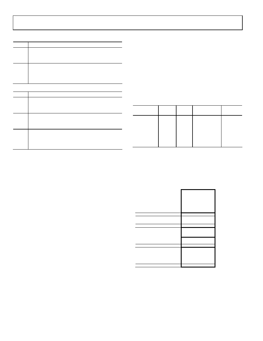
RESET AND REMAP
The ARM exception vectors are all situated at the bottom of the
memory array, from Address 0x00000000 to Address 0x00000020,
as shown in Figure 40.
KERNEL
INTERRUPT
SERVICE ROUTINES
INTERRUPT
SERVICE ROUTINES
ARM EXCEPTION
VECTOR ADDRESSES
0x00000020
0x00047FFF
0x0009F800
0xFFFFFFFF
FLASH/EE
SRAM
MIRROR SPACE
0x00000000 0x00000000
0x00040000
0x00080000
09123
-02
7
Figure 40. Remap for Exception Execution
By default, and after any reset, the Flash/EE is mirrored at the
bottom of the memory array. The remap function allows the
programmer to mirror the SRAM at the bottom of the memory
array, which facilitates execution of exception routines from
SRAM instead of from Flash/EE. This means exceptions are
executed twice as fast, being executed in 32-bit ARM mode with
32-bit wide SRAM instead of 16-bit wide Flash/EE memory.
相关PDF资料 |
PDF描述 |
|---|---|
| REC5-243.3SRWZ/H4/A | CONV DC/DC 5W 9-36VIN 3.3VOUT |
| EVAL-ADUC7023QSPZ | KIT DEV FOR ADUC7023 QUICK START |
| RPS-1K-6-250/2.0-9 | HEAT SHRINK SLEEVE |
| ECM30DCWH | CONN EDGECARD 60POS DIP .156 SLD |
| SC43B-3R3 | INDUCTOR SMD 3.3UH 1.44A 7.96MHZ |
相关代理商/技术参数 |
参数描述 |
|---|---|
| EVAL-ADUC7128QSPZ | 功能描述:KIT DEV FOR ADUC7128 RoHS:是 类别:编程器,开发系统 >> 通用嵌入式开发板和套件(MCU、DSP、FPGA、CPLD等) 系列:QuickStart™ PLUS 套件 产品培训模块:Blackfin® Processor Core Architecture Overview Blackfin® Device Drivers Blackfin® Optimizations for Performance and Power Consumption Blackfin® System Services 特色产品:Blackfin? BF50x Series Processors 标准包装:1 系列:Blackfin® 类型:DSP 适用于相关产品:ADSP-BF548 所含物品:板,软件,4x4 键盘,光学拨轮,QVGA 触摸屏 LCD 和 40G 硬盘 配用:ADZS-BFBLUET-EZEXT-ND - EZ-EXTENDER DAUGHTERBOARDADZS-BFLLCD-EZEXT-ND - BOARD EXT LANDSCAP LCD INTERFACE 相关产品:ADSP-BF542BBCZ-4A-ND - IC DSP 16BIT 400MHZ 400CSBGAADSP-BF544MBBCZ-5M-ND - IC DSP 16BIT 533MHZ MDDR 400CBGAADSP-BF542MBBCZ-5M-ND - IC DSP 16BIT 533MHZ MDDR 400CBGAADSP-BF542KBCZ-6A-ND - IC DSP 16BIT 600MHZ 400CSBGAADSP-BF547MBBCZ-5M-ND - IC DSP 16BIT 533MHZ MDDR 400CBGAADSP-BF548BBCZ-5A-ND - IC DSP 16BIT 533MHZ 400CSBGAADSP-BF547BBCZ-5A-ND - IC DSP 16BIT 533MHZ 400CSBGAADSP-BF544BBCZ-5A-ND - IC DSP 16BIT 533MHZ 400CSBGAADSP-BF542BBCZ-5A-ND - IC DSP 16BIT 533MHZ 400CSBGA |
| EVAL-ADUC7128QSPZ2 | 制造商:AD 制造商全称:Analog Devices 功能描述:Precision Analog Microcontroller ARM7TDMI MCU with 12-Bit ADC and DDS DAC |
| EVAL-ADUC7129QSPZ | 制造商:Analog Devices 功能描述:- Bulk |
| EVAL-ADUC812QS | 制造商:Analog Devices 功能描述:DEVELOPMENT KIT SYSTEM |
| EVAL-ADUC812QSP | 制造商:AD 制造商全称:Analog Devices 功能描述:MicroConverter㈢, Multichannel 12-Bit ADC with Embedded Flash MCU |
发布紧急采购,3分钟左右您将得到回复。