- 您现在的位置:买卖IC网 > PDF目录17109 > EVAL-ADUC7126QSPZ (Analog Devices Inc)BOARD EVALUATION FOR ADUC7126 PDF资料下载
参数资料
| 型号: | EVAL-ADUC7126QSPZ |
| 厂商: | Analog Devices Inc |
| 文件页数: | 63/108页 |
| 文件大小: | 0K |
| 描述: | BOARD EVALUATION FOR ADUC7126 |
| 设计资源: | EVAL-ADUC7126 Schematic ADUC7126 Gerber Files |
| 标准包装: | 1 |
| 系列: | MicroConverter® ADuC7xxx |
| 类型: | MCU |
| 适用于相关产品: | ADUC7126 |
| 所含物品: | 板 |
第1页第2页第3页第4页第5页第6页第7页第8页第9页第10页第11页第12页第13页第14页第15页第16页第17页第18页第19页第20页第21页第22页第23页第24页第25页第26页第27页第28页第29页第30页第31页第32页第33页第34页第35页第36页第37页第38页第39页第40页第41页第42页第43页第44页第45页第46页第47页第48页第49页第50页第51页第52页第53页第54页第55页第56页第57页第58页第59页第60页第61页第62页当前第63页第64页第65页第66页第67页第68页第69页第70页第71页第72页第73页第74页第75页第76页第77页第78页第79页第80页第81页第82页第83页第84页第85页第86页第87页第88页第89页第90页第91页第92页第93页第94页第95页第96页第97页第98页第99页第100页第101页第102页第103页第104页第105页第106页第107页第108页
ADuC7124/ADuC7126
Data Sheet
Rev. C | Page 58 of 108
DIGITAL PERIPHERAL
GENERAL-PURPOSE INPUT/OUTPUT
The ADuC7124/ADuC7126 provide 40 general-purpose, bidirec-
tional I/O (GPIO) pins. All I/O pins are 5 V tolerant, meaning
the GPIOs support an input voltage of 5 V.
In general, many of the GPIO pins have multiple functions (see
the Pin Configurations and Function Descriptions section for
pin function definitions). By default, the GPIO pins are configured
in GPIO mode.
All GPIO pins have an internal pull-up resistor (of about 100 kΩ),
and their drive capability is 1.6 mA. Note that a maximum of
20 GPIOs can drive 1.6 mA at the same time. Using the GPxPAR
registers, it is possible to enable/disable the pull-up resistors for
the following ports: P0.0, P0.4, P0.5, P0.6, P0.7, and the eight
GPIOs of P1.
The 40 GPIOs are grouped in five ports, Port 0 to Port 4 (Port x).
Each port is controlled by four or five MMRs.
Note that the kernel changes P0.6 from its default configuration
at reset (MRST) to GPIO mode. If MRST is used for external
circuitry, an external pull-up resistor should be used to ensure
that the level on P0.6 does not drop when the kernel switches
mode. Otherwise, P0.6 goes low for the reset period. For example,
if MRST is required for power-down, it can be reconfigured in
GP0CON MMR.
The input level of any GPIO can be read at any time in the
GPxDAT MMR, even when the pin is configured in a mode
other than GPIO. The PLA input is always active.
When the ADuC7124/ADuC7126 enter a power-saving mode,
the GPIO pins retain their state. Also, note that, by setting
RSTCFG Bit 0, the GPIO pins can retain their state during a
watchdog or software reset.
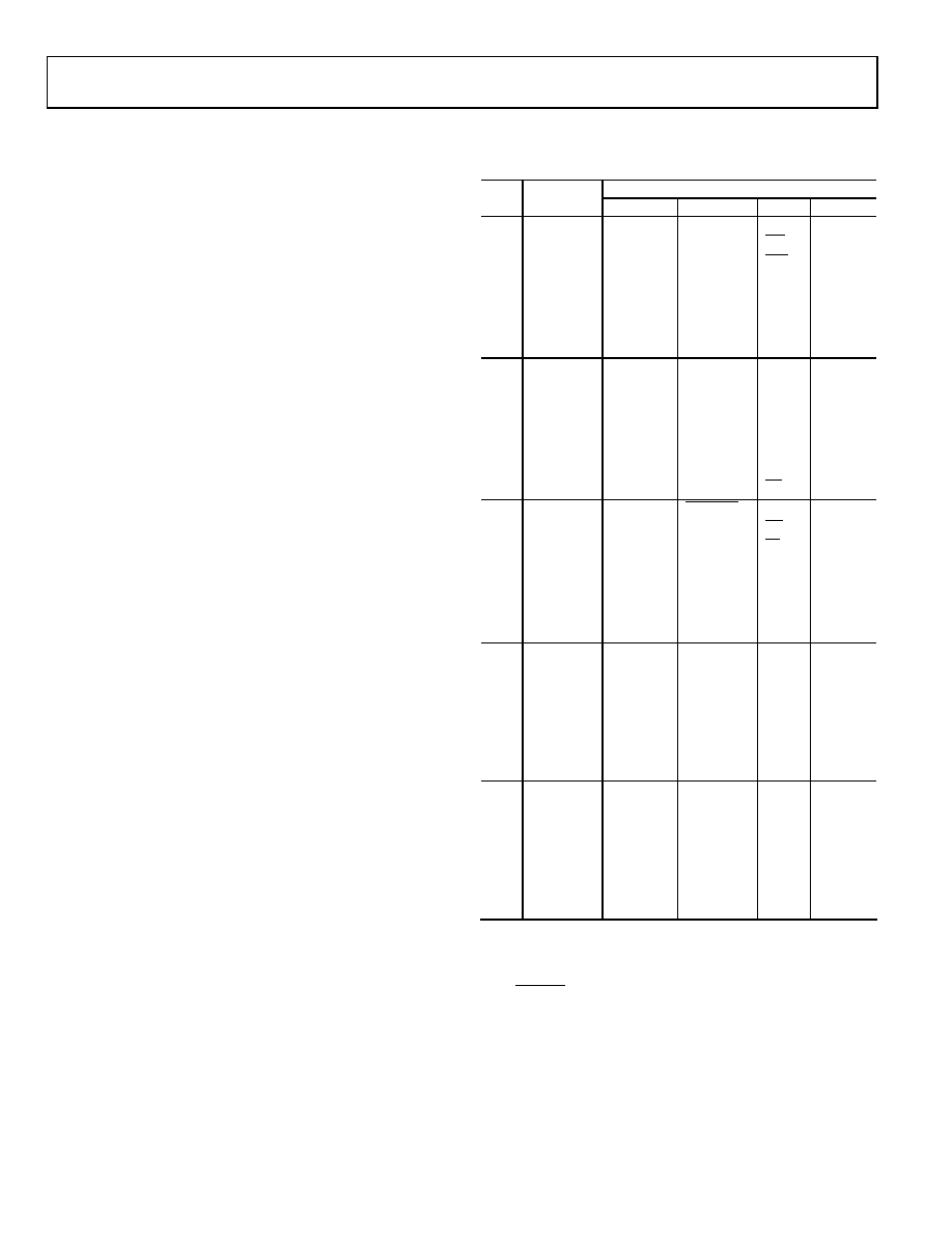
Table 78. GPIO Pin Function Descriptions
Configuration
Port
Pin
00
01
10
11
0
BM/P0.0
GPIO
CMP
MS0
PLAI[7]
TDI/P0.11
GPIO/JTAG
PWM4
BLE5
GPIO/JTAG
PWM5
GPIO/JTAG
TRST
ADCBUSY
P0.4
GPIO/IRQ0
PWMTRIP
PLAO[1]
P0.5
GPIO/IRQ1
ADCBUSY
PLAO[2]
P0.6
GPIO
MRST
PLAO[3]
P0.7
GPIO
ECLK/XCLK2
SIN0
PLAO[4]
1
P1.0
GPIO/T1
SIN0
PLAI[0]
P1.1
GPIO
SOUT0
PLAI[1]
P1.2
GPIO
PLAI[2]
P1.3
GPIO
PLAI[3]
P1.4
GPIO/IRQ2
PLAI[4]
P1.5
GPIO/IRQ3
PLAI[5]
P1.6
GPIO
PLAI[6]
P1.7
GPIO
PLAO[0]
2
P2.0
GPIO
CONVSTART4
SOUT0
PLAO[5]
P2.1
GPIO
PWM0
PLAO[6]
P2.2
GPIO
PWM1
RS5
PLAO[7]
P2.3
GPIO
SIN1
P2.4
GPIO
PWM0
SOUT1
P2.5
GPIO
PWM1
P2.6
GPIO
PWM2
P2.7
GPIO
PWM3
3
P3.0
GPIO
PWM0
AD05
PLAI[8]
P3.1
GPIO
PWM1
AD15
PLAI[9]
P3.2
GPIO
PWM2
AD25
PLAI[10]
P3.3
GPIO
PWM3
AD35
PLAI[11]
P3.4
GPIO
PWM4
AD45
PLAI[12]
P3.5
GPIO
PWM5
AD55
PLAI[13]
P3.6
GPIO
PWMTRIP
AD65
PLAI[14]
P3.7
GPIO
PWMSYNC
AD75
PLAI[15]
4
P4.0
GPIO
SIN1
AD85
PLAO[8]
P4.1
GPIO
SOUT1
AD95
PLAO[9]
P4.2
GPIO
PLAO[10]
P4.3
GPIO
PLAO[11]
P4.4
GPIO
PLAO[12]
P4.5
GPIO/RTCK
PLAO[13]
P4.6
GPIO
PLAO[14]
P4.7
GPIO
PLAO[15]
1 These pins should not be used by user code .
2 When configured in Mode 1, P0.7 is ECLK by default, or core clock output. To
configure it as a clock input, the MDCLK bits in PLLCON must be set to 11.
3 See Table 90 for SPM configurations.
4 The CONVSTART signal is active in all modes of P2.0.
5 External Memory Interface signals are only available on ADuC7126.
相关PDF资料 |
PDF描述 |
|---|---|
| REC5-243.3SRWZ/H4/A | CONV DC/DC 5W 9-36VIN 3.3VOUT |
| EVAL-ADUC7023QSPZ | KIT DEV FOR ADUC7023 QUICK START |
| RPS-1K-6-250/2.0-9 | HEAT SHRINK SLEEVE |
| ECM30DCWH | CONN EDGECARD 60POS DIP .156 SLD |
| SC43B-3R3 | INDUCTOR SMD 3.3UH 1.44A 7.96MHZ |
相关代理商/技术参数 |
参数描述 |
|---|---|
| EVAL-ADUC7128QSPZ | 功能描述:KIT DEV FOR ADUC7128 RoHS:是 类别:编程器,开发系统 >> 通用嵌入式开发板和套件(MCU、DSP、FPGA、CPLD等) 系列:QuickStart™ PLUS 套件 产品培训模块:Blackfin® Processor Core Architecture Overview Blackfin® Device Drivers Blackfin® Optimizations for Performance and Power Consumption Blackfin® System Services 特色产品:Blackfin? BF50x Series Processors 标准包装:1 系列:Blackfin® 类型:DSP 适用于相关产品:ADSP-BF548 所含物品:板,软件,4x4 键盘,光学拨轮,QVGA 触摸屏 LCD 和 40G 硬盘 配用:ADZS-BFBLUET-EZEXT-ND - EZ-EXTENDER DAUGHTERBOARDADZS-BFLLCD-EZEXT-ND - BOARD EXT LANDSCAP LCD INTERFACE 相关产品:ADSP-BF542BBCZ-4A-ND - IC DSP 16BIT 400MHZ 400CSBGAADSP-BF544MBBCZ-5M-ND - IC DSP 16BIT 533MHZ MDDR 400CBGAADSP-BF542MBBCZ-5M-ND - IC DSP 16BIT 533MHZ MDDR 400CBGAADSP-BF542KBCZ-6A-ND - IC DSP 16BIT 600MHZ 400CSBGAADSP-BF547MBBCZ-5M-ND - IC DSP 16BIT 533MHZ MDDR 400CBGAADSP-BF548BBCZ-5A-ND - IC DSP 16BIT 533MHZ 400CSBGAADSP-BF547BBCZ-5A-ND - IC DSP 16BIT 533MHZ 400CSBGAADSP-BF544BBCZ-5A-ND - IC DSP 16BIT 533MHZ 400CSBGAADSP-BF542BBCZ-5A-ND - IC DSP 16BIT 533MHZ 400CSBGA |
| EVAL-ADUC7128QSPZ2 | 制造商:AD 制造商全称:Analog Devices 功能描述:Precision Analog Microcontroller ARM7TDMI MCU with 12-Bit ADC and DDS DAC |
| EVAL-ADUC7129QSPZ | 制造商:Analog Devices 功能描述:- Bulk |
| EVAL-ADUC812QS | 制造商:Analog Devices 功能描述:DEVELOPMENT KIT SYSTEM |
| EVAL-ADUC812QSP | 制造商:AD 制造商全称:Analog Devices 功能描述:MicroConverter㈢, Multichannel 12-Bit ADC with Embedded Flash MCU |
发布紧急采购,3分钟左右您将得到回复。