参数资料
| 型号: | XCV405E-8FG676C |
| 厂商: | Xilinx Inc |
| 文件页数: | 77/118页 |
| 文件大小: | 0K |
| 描述: | IC FPGA 1.8V C-TEMP 676-FBGA |
| 产品变化通告: | FPGA Family Discontinuation 18/Apr/2011 |
| 标准包装: | 1 |
| 系列: | Virtex®-E EM |
| LAB/CLB数: | 2400 |
| 逻辑元件/单元数: | 10800 |
| RAM 位总计: | 573440 |
| 输入/输出数: | 404 |
| 门数: | 129600 |
| 电源电压: | 1.71 V ~ 1.89 V |
| 安装类型: | 表面贴装 |
| 工作温度: | 0°C ~ 85°C |
| 封装/外壳: | 676-BGA |
| 供应商设备封装: | 676-FBGA(27x27) |
第1页第2页第3页第4页第5页第6页第7页第8页第9页第10页第11页第12页第13页第14页第15页第16页第17页第18页第19页第20页第21页第22页第23页第24页第25页第26页第27页第28页第29页第30页第31页第32页第33页第34页第35页第36页第37页第38页第39页第40页第41页第42页第43页第44页第45页第46页第47页第48页第49页第50页第51页第52页第53页第54页第55页第56页第57页第58页第59页第60页第61页第62页第63页第64页第65页第66页第67页第68页第69页第70页第71页第72页第73页第74页第75页第76页当前第77页第78页第79页第80页第81页第82页第83页第84页第85页第86页第87页第88页第89页第90页第91页第92页第93页第94页第95页第96页第97页第98页第99页第100页第101页第102页第103页第104页第105页第106页第107页第108页第109页第110页第111页第112页第113页第114页第115页第116页第117页第118页
Virtex-E 1.8 V Extended Memory Field Programmable Gate Arrays
DS025-3 (v3.0) March 21, 2014
Module 3 of 4
5
R
— OBSOLETE — OBSOLETE — OBSOLETE — OBSOLETE —
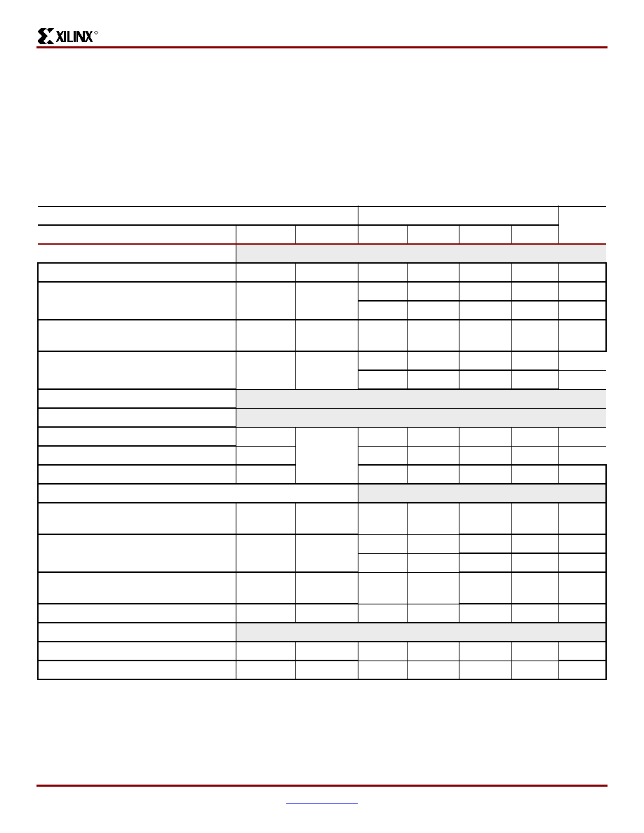
Virtex-E Switching Characteristics
All devices are 100% functionally tested. Internal timing parameters are derived from measuring internal test patterns. Listed
below are representative values. For more specific, more precise, and worst-case guaranteed data, use the values reported
by the static timing analyzer (TRCE in the Xilinx Development System) and back-annotated to the simulation net list. All
timing parameters assume worst-case operating conditions (supply voltage and junction temperature). Values apply to all
Virtex-E devices unless otherwise noted.
IOB Input Switching Characteristics
Input delays associated with the pad are specified for LVTTL levels. For other standards, adjust the delays with the values
Speed Grade(2)
Units
Description(1)
Symbol
Device
Min
-8
-7
-6
Propagation Delays
Pad to I output, no delay
TIOPI
All
0.43
0.8
ns, max
Pad to I output, with delay
TIOPID
XCV405E
0.51
1.0
ns, max
XCV812E
0.55
1.1
ns, max
Pad to output IQ via transparent latch,
no delay
TIOPLI
All
0.75
1.4
1.5
1.6
ns, max
Pad to output IQ via transparent latch,
with delay
TIOPLID
XCV405E
1.55
3.5
3.6
3.7
ns, max
XCV812E
1.55
3.5
3.6
3.7
ns, max
Propagation Delays
Clock
Minimum Pulse Width, High
TCH
All
0.56
1.2
1.3
1.4
ns, min
Minimum Pulse Width, Low
TCL
0.56
1.2
1.3
1.4
ns, min
Clock CLK to output IQ
TIOCKIQ
0.18
0.4
0.7
ns, max
Setup and Hold Times with respect to Clock at IOB Input Register
Pad, no delay
TIOPICK /
TIOICKP
All
0.69 / 0
1.3 / 0
1.4 / 0
1.5 / 0
ns, min
Pad, with delay
TIOPICKD /
TIOICKPD
XCV405E
1.49 / 0
3.4 / 0
3.5 / 0
ns, min
XCV812E
1.49 / 0
3.4 / 0
3.5 / 0
ns, min
ICE input
TIOICECK /
TIOCKICE
All
0.28 /
0.0
0.55 /
0.01
0.7 /
0.01
0.7 /
0.01
ns, min
SR input (IFF, synchronous)
TIOSRCKI
All
0.38
0.8
0.9
1.0
ns, min
Set/Reset Delays
SR input to IQ (asynchronous)
TIOSRIQ
All
0.54
1.1
1.2
1.4
ns, max
GSR to output IQ
TGSRQ
All
3.88
7.6
8.5
9.7
ns, max
Notes:
1.
A Zero “0” Hold Time listing indicates no hold time or a negative hold time. Negative values can not be guaranteed “best-case”, but
if a “0” is listed, there is no positive hold time.
2.
Input timing i for LVTTL is measured at 1.4 V. For other I/O standards, see Table 3.
相关PDF资料 |
PDF描述 |
|---|---|
| XCV405E-7FG676I | IC FPGA 1.8V 676-BGA |
| XC6VLX195T-1FFG784C | IC FPGA VIRTEX 6 199K 784FFGBGA |
| XC6VCX130T-2FFG784I | IC FPGA VIRTEX 6 128K 784FFGBGA |
| XC4VLX60-11FF668I | IC FPGA VIRTEX-4LX 668FFBGA |
| XC4VLX60-12FFG668C | IC FPGA VIRTEX-4 LX 60K 668FCBGA |
相关代理商/技术参数 |
参数描述 |
|---|---|
| XCV405E-8FG676I | 制造商:XILINX 制造商全称:XILINX 功能描述:Virtex-E 1.8 V Extended Memory Field Programmable Gate Arrays |
| XCV405E-8FG900C | 制造商:XILINX 制造商全称:XILINX 功能描述:Virtex-E 1.8 V Extended Memory Field Programmable Gate Arrays |
| XCV405E-8FG900I | 制造商:XILINX 制造商全称:XILINX 功能描述:Virtex-E 1.8 V Extended Memory Field Programmable Gate Arrays |
| XCV50 | 制造商:XILINX 制造商全称:XILINX 功能描述:Field Programmable Gate Arrays |
| XCV50-4BG256C | 功能描述:IC FPGA 2.5V C-TEMP 256-PBGA RoHS:否 类别:集成电路 (IC) >> 嵌入式 - FPGA(现场可编程门阵列) 系列:Virtex® 标准包装:1 系列:Kintex-7 LAB/CLB数:25475 逻辑元件/单元数:326080 RAM 位总计:16404480 输入/输出数:350 门数:- 电源电压:0.97 V ~ 1.03 V 安装类型:表面贴装 工作温度:0°C ~ 85°C 封装/外壳:900-BBGA,FCBGA 供应商设备封装:900-FCBGA(31x31) 其它名称:122-1789 |
发布紧急采购,3分钟左右您将得到回复。