参数资料
| 型号: | XCV405E-8FG676C |
| 厂商: | Xilinx Inc |
| 文件页数: | 2/118页 |
| 文件大小: | 0K |
| 描述: | IC FPGA 1.8V C-TEMP 676-FBGA |
| 产品变化通告: | FPGA Family Discontinuation 18/Apr/2011 |
| 标准包装: | 1 |
| 系列: | Virtex®-E EM |
| LAB/CLB数: | 2400 |
| 逻辑元件/单元数: | 10800 |
| RAM 位总计: | 573440 |
| 输入/输出数: | 404 |
| 门数: | 129600 |
| 电源电压: | 1.71 V ~ 1.89 V |
| 安装类型: | 表面贴装 |
| 工作温度: | 0°C ~ 85°C |
| 封装/外壳: | 676-BGA |
| 供应商设备封装: | 676-FBGA(27x27) |
第1页当前第2页第3页第4页第5页第6页第7页第8页第9页第10页第11页第12页第13页第14页第15页第16页第17页第18页第19页第20页第21页第22页第23页第24页第25页第26页第27页第28页第29页第30页第31页第32页第33页第34页第35页第36页第37页第38页第39页第40页第41页第42页第43页第44页第45页第46页第47页第48页第49页第50页第51页第52页第53页第54页第55页第56页第57页第58页第59页第60页第61页第62页第63页第64页第65页第66页第67页第68页第69页第70页第71页第72页第73页第74页第75页第76页第77页第78页第79页第80页第81页第82页第83页第84页第85页第86页第87页第88页第89页第90页第91页第92页第93页第94页第95页第96页第97页第98页第99页第100页第101页第102页第103页第104页第105页第106页第107页第108页第109页第110页第111页第112页第113页第114页第115页第116页第117页第118页
Virtex-E 1.8 V Extended Memory Field Programmable Gate Arrays
Module 2 of 4
DS025-2 (v3.0) March 21, 2014
6
R
— OBSOLETE — OBSOLETE — OBSOLETE — OBSOLETE —
Table 5 shows the depth and width aspect ratios for the
block SelectRAM. The Virtex-E block SelectRAM also
includes dedicated routing to provide an efficient interface
with both CLBs and other block SelectRAM modules. Refer
to XAPP130 for block SelectRAM timing waveforms.
Programmable Routing Matrix
It is the longest delay path that limits the speed of any
worst-case design. Consequently, the Virtex-E routing
architecture and its place-and-route software were defined
in a joint optimization process. This joint optimization mini-
mizes long-path delays, and consequently, yields the best
system performance.
The joint optimization also reduces design compilation
times because the architecture is software-friendly. Design
cycles are correspondingly reduced due to shorter design
iteration times.
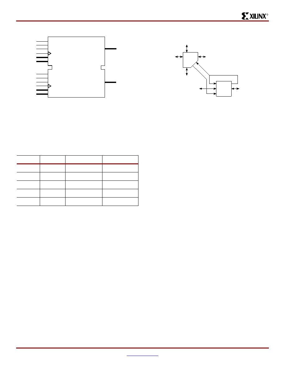
Local Routing
The VersaBlock, shown in Figure 7, provides local routing
resources with the following types of connections:
Interconnections among the LUTs, flip-flops, and GRM
Internal CLB feedback paths that provide high-speed
connections to LUTs within the same CLB, chaining
them together with minimal routing delay
Direct paths that provide high-speed connections
between horizontally adjacent CLBs, eliminating the
delay of the GRM
.
General Purpose Routing
Most Virtex-E signals are routed on the general purpose
routing, and consequently, the majority of interconnect
resources are associated with this level of the routing hier-
archy. The general routing resources are located in horizon-
tal and vertical routing channels associated with the CLB
rows and columns. The general-purpose routing resources
are listed below.
Adjacent to each CLB is a General Routing Matrix
(GRM). The GRM is the switch matrix through which
horizontal and vertical routing resources connect, and
is also the means by which the CLB gains access to
the general purpose routing.
24 single-length lines route GRM signals to adjacent
GRMs in each of the four directions.
72 buffered Hex lines route GRM signals to another
GRMs six-blocks away in each one of the four
directions. Organized in a staggered pattern, Hex lines
are driven only at their endpoints. Hex-line signals can
be accessed either at the endpoints or at the midpoint
(three blocks from the source). One third of the Hex
lines are bidirectional, while the remaining ones are
uni-directional.
12 Longlines are buffered, bidirectional wires that
distribute signals across the device quickly and
efficiently. Vertical Longlines span the full height of the
device, and horizontal ones span the full width of the
device.
I/O Routing
Virtex-E devices have additional routing resources around
their periphery that form an interface between the CLB array
and the IOBs. This additional routing, called the VersaRing,
facilitates pin-swapping and pin-locking, such that logic
redesigns can adapt to existing PCB layouts. Time-to-mar-
ket is reduced, since PCBs and other system components
can be manufactured while the logic design is still in prog-
ress.
Figure 6: Dual-Port Block SelectRAM
Table 5:
Block SelectRAM Port Aspect Ratios
Width
Depth
ADDR Bus
Data Bus
1
4096
ADDR<11:0>
DATA<0>
2
2048
ADDR<10:0>
DATA<1:0>
4
1024
ADDR<9:0>
DATA<3:0>
8
512
ADDR<8:0>
DATA<7:0>
16
256
ADDR<7:0>
DATA<15:0>
WEB
ENB
RSTB
CLKB
ADDRB[#:0]
DIB[#:0]
WEA
ENA
RSTA
CLKA
ADDRA[#:0]
DIA[#:0]
DOA[#:0]
DOB[#:0]
RAMB4_S#_S#
ds022_06_121699
Figure 7: Virtex-E Local Routing
XCVE_ds_007
CLB
GRM
To
Adjacent
GRM
To Adjacent
GRM
Direct
Connection
To Adjacent
CLB
To Adjacent
GRM
To Adjacent
GRM
Direct Connection
To Adjacent
CLB
相关PDF资料 |
PDF描述 |
|---|---|
| XCV405E-7FG676I | IC FPGA 1.8V 676-BGA |
| XC6VLX195T-1FFG784C | IC FPGA VIRTEX 6 199K 784FFGBGA |
| XC6VCX130T-2FFG784I | IC FPGA VIRTEX 6 128K 784FFGBGA |
| XC4VLX60-11FF668I | IC FPGA VIRTEX-4LX 668FFBGA |
| XC4VLX60-12FFG668C | IC FPGA VIRTEX-4 LX 60K 668FCBGA |
相关代理商/技术参数 |
参数描述 |
|---|---|
| XCV405E-8FG676I | 制造商:XILINX 制造商全称:XILINX 功能描述:Virtex-E 1.8 V Extended Memory Field Programmable Gate Arrays |
| XCV405E-8FG900C | 制造商:XILINX 制造商全称:XILINX 功能描述:Virtex-E 1.8 V Extended Memory Field Programmable Gate Arrays |
| XCV405E-8FG900I | 制造商:XILINX 制造商全称:XILINX 功能描述:Virtex-E 1.8 V Extended Memory Field Programmable Gate Arrays |
| XCV50 | 制造商:XILINX 制造商全称:XILINX 功能描述:Field Programmable Gate Arrays |
| XCV50-4BG256C | 功能描述:IC FPGA 2.5V C-TEMP 256-PBGA RoHS:否 类别:集成电路 (IC) >> 嵌入式 - FPGA(现场可编程门阵列) 系列:Virtex® 标准包装:1 系列:Kintex-7 LAB/CLB数:25475 逻辑元件/单元数:326080 RAM 位总计:16404480 输入/输出数:350 门数:- 电源电压:0.97 V ~ 1.03 V 安装类型:表面贴装 工作温度:0°C ~ 85°C 封装/外壳:900-BBGA,FCBGA 供应商设备封装:900-FCBGA(31x31) 其它名称:122-1789 |
发布紧急采购,3分钟左右您将得到回复。