参数资料
| 型号: | XCV405E-8FG676C |
| 厂商: | Xilinx Inc |
| 文件页数: | 33/118页 |
| 文件大小: | 0K |
| 描述: | IC FPGA 1.8V C-TEMP 676-FBGA |
| 产品变化通告: | FPGA Family Discontinuation 18/Apr/2011 |
| 标准包装: | 1 |
| 系列: | Virtex®-E EM |
| LAB/CLB数: | 2400 |
| 逻辑元件/单元数: | 10800 |
| RAM 位总计: | 573440 |
| 输入/输出数: | 404 |
| 门数: | 129600 |
| 电源电压: | 1.71 V ~ 1.89 V |
| 安装类型: | 表面贴装 |
| 工作温度: | 0°C ~ 85°C |
| 封装/外壳: | 676-BGA |
| 供应商设备封装: | 676-FBGA(27x27) |
第1页第2页第3页第4页第5页第6页第7页第8页第9页第10页第11页第12页第13页第14页第15页第16页第17页第18页第19页第20页第21页第22页第23页第24页第25页第26页第27页第28页第29页第30页第31页第32页当前第33页第34页第35页第36页第37页第38页第39页第40页第41页第42页第43页第44页第45页第46页第47页第48页第49页第50页第51页第52页第53页第54页第55页第56页第57页第58页第59页第60页第61页第62页第63页第64页第65页第66页第67页第68页第69页第70页第71页第72页第73页第74页第75页第76页第77页第78页第79页第80页第81页第82页第83页第84页第85页第86页第87页第88页第89页第90页第91页第92页第93页第94页第95页第96页第97页第98页第99页第100页第101页第102页第103页第104页第105页第106页第107页第108页第109页第110页第111页第112页第113页第114页第115页第116页第117页第118页
Virtex-E 1.8 V Extended Memory Field Programmable Gate Arrays
DS025-2 (v3.0) March 21, 2014
Module 2 of 4
17
R
— OBSOLETE — OBSOLETE — OBSOLETE — OBSOLETE —
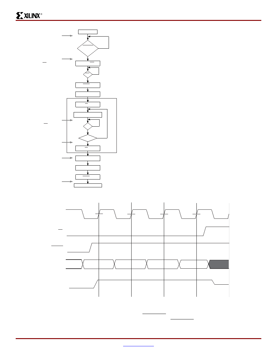
Boundary-Scan Mode
In the boundary-scan mode, configuration is done through
the IEEE 1149.1 Test Access Port. Note that the
PROGRAM pin must be pulled High prior to reconfiguration.
A Low on the PROGRAM pin resets the TAP controller and
no JTAG operations can be performed.
Figure 18: SelectMAP Flowchart for Write Operations
Apply Power
Release INIT
If used to delay
configuration
On first FPGA
PROGRAM
from Low
to High
Set WRITE = Low
Enter Data Source
Set CS = Low
On first FPGA
Set CS = High
Apply Configuration Byte
INIT?
High
Low
Yes
No
Busy?
Low
High
Disable Data Source
Set WRITE = High
When all DONE pins
are released, DONE goes High
and start-up sequences complete.
If no errors,
later FPGAs enter start-up phase
releasing DONE.
If no errors,
first FPGAs enter start-up phase
releasing DONE.
Once per bitstream,
FPGA checks data using CRC
and pulls INIT Low on error.
FPGA makes a final
clearing pass and releases
INIT when finished.
FPGA starts to clear
configuration memory.
For any other FPGAs
ds003_17_090602
Repeat Sequence A
Configuration Completed
Sequence A
End of Data?
Yes
No
Figure 19: SelectMAP Write Abort Waveforms
CCLK
CS
WRITE
Abort
DATA[0:7]
BUSY
DS022_46_071702
相关PDF资料 |
PDF描述 |
|---|---|
| XCV405E-7FG676I | IC FPGA 1.8V 676-BGA |
| XC6VLX195T-1FFG784C | IC FPGA VIRTEX 6 199K 784FFGBGA |
| XC6VCX130T-2FFG784I | IC FPGA VIRTEX 6 128K 784FFGBGA |
| XC4VLX60-11FF668I | IC FPGA VIRTEX-4LX 668FFBGA |
| XC4VLX60-12FFG668C | IC FPGA VIRTEX-4 LX 60K 668FCBGA |
相关代理商/技术参数 |
参数描述 |
|---|---|
| XCV405E-8FG676I | 制造商:XILINX 制造商全称:XILINX 功能描述:Virtex-E 1.8 V Extended Memory Field Programmable Gate Arrays |
| XCV405E-8FG900C | 制造商:XILINX 制造商全称:XILINX 功能描述:Virtex-E 1.8 V Extended Memory Field Programmable Gate Arrays |
| XCV405E-8FG900I | 制造商:XILINX 制造商全称:XILINX 功能描述:Virtex-E 1.8 V Extended Memory Field Programmable Gate Arrays |
| XCV50 | 制造商:XILINX 制造商全称:XILINX 功能描述:Field Programmable Gate Arrays |
| XCV50-4BG256C | 功能描述:IC FPGA 2.5V C-TEMP 256-PBGA RoHS:否 类别:集成电路 (IC) >> 嵌入式 - FPGA(现场可编程门阵列) 系列:Virtex® 标准包装:1 系列:Kintex-7 LAB/CLB数:25475 逻辑元件/单元数:326080 RAM 位总计:16404480 输入/输出数:350 门数:- 电源电压:0.97 V ~ 1.03 V 安装类型:表面贴装 工作温度:0°C ~ 85°C 封装/外壳:900-BBGA,FCBGA 供应商设备封装:900-FCBGA(31x31) 其它名称:122-1789 |
发布紧急采购,3分钟左右您将得到回复。