- 您现在的位置:买卖IC网 > PDF目录202515 > VNC1L-1A (Future Technology Devices International Ltd) PDF资料下载
参数资料
| 型号: | VNC1L-1A |
| 厂商: | Future Technology Devices International Ltd |
| 元件分类: | 总线控制器 |
| 中文描述: | UNIVERSAL SERIAL BUS CONTROLLER, PQFP48 |
| 封装: | 7 X 7 MM, 0.50 MM PITCH, GREEN, LQFP-48 |
| 文件页数: | 32/32页 |
| 文件大小: | 672K |
| 代理商: | VNC1L-1A |
第1页第2页第3页第4页第5页第6页第7页第8页第9页第10页第11页第12页第13页第14页第15页第16页第17页第18页第19页第20页第21页第22页第23页第24页第25页第26页第27页第28页第29页第30页第31页当前第32页
Copyright 2009 Future Technology Devices International Limited
9
Document Reference No.: FT_000030
Vinculum VNC1L Embedded USB Host Controller IC Datasheet Version 2.02
Clearance No.: FTDI# 50
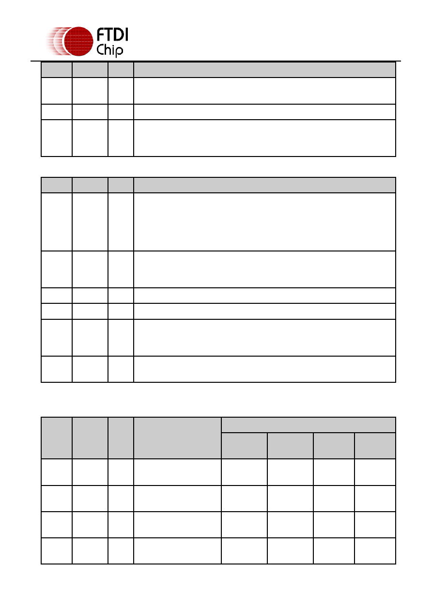
Pin No.
Name
Type
Description
3
AVCC
PWR
+3.3V supply to the internal clock multiplier. This pin requires a 100nF decoupling
capacitor
6
AGND
PWR
Device analogue ground supply for internal clock multiplier
17, 30,
40
VCCIO
PWR
+3.3V supply to the ADBUS, ACBUS, BDBUS and BCBUS Interface pins (11..16,
18..23, 31..38, 41..48). Leaving the VCCIO unconnected will lead to unpredictable
operation on these interface pins.
Table 3.2 Power and Ground Group
Pin No.
Name
Type
Description
4
XTIN
Input
Input to 12MHz Oscillator Cell. Connect 12MHz crystal across pins 4 and 5, with
suitable loading capacitors to GND. This pin can also be driven by an external 12MHz
clock signal. Note that the switching threshold of this pin is VCC/2, so if driving from
an external source, the source must be driving at +3.3V CMOS level or AC coupled to
centre around VCC/2
5
XTOUT
Outpu
t
Output from 12MHz Oscillator Cell. Connect 12MHz crystal across pins 4 and 5, with
suitable loading capacitors to GND. XTOUT stops oscillating during USB suspend, so
take care using this signal to clock external logic
7
PLLFLTR
Input
External PLL filter circuit input. RC filter circuit must be fitted on this pin
8
TEST
Input
Puts the device into IC test mode. Must be tied to GND for normal operation
9
RESET#
Input
Can be used by an external device to reset VNC1L. This pin can be used in
combination with PROG# and the UART interface to program firmware into VNC1L. If
not required pull-up to VCC via a 47k resistor.*
10
PROG#
Input
This pin is used in combination with the RESET# pin and the UART interface to
program firmware into VNC1L.*
Table 3.3 Miscellaneous Signal Group
* These pins are pulled to VCC via internal 200k resistors.
Pin No.
Name
Type
Description
Combined Interface Mode
UART
Interface
Parallel FIFO
Interface
SPI Slave
Interface
I/O Port
11
BDBUS0
I/O
5V safe bidirectional
data/control bus, BD bit 0
PortBD0
12
BDBUS1
I/O
5V safe bidirectional
data/control bus, BD bit 1
PortBD1
13
BDBUS2
I/O
5V safe bidirectional
data/control bus, BD bit 2
PortBD2
14
BDBUS3
I/O
5V safe bidirectional
data/control bus, BD bit 3
PortBD3
相关PDF资料 |
PDF描述 |
|---|---|
| VND5E012AYTR-E | SPECIALTY ANALOG CIRCUIT, PDSO36 |
| VNL5050S5-E | POWER SUPPLY SUPPORT CKT, PDSO8 |
| VNL5050N3TR-E | POWER SUPPLY SUPPORT CKT, PDSO3 |
| VO27.0000000M0000001 | VCXO, CLOCK, 27 MHz, TTL OUTPUT |
| VP06DDC1R0N999 | 0.3 W, SMPS TRANSFORMER |
相关代理商/技术参数 |
参数描述 |
|---|---|
| VNC1L-1A-REEL | 功能描述:USB 接口集成电路 USB Vinculum Host /Dev Ctrl IC LQFP-48 RoHS:否 制造商:Cypress Semiconductor 产品:USB 2.0 数据速率: 接口类型:SPI 工作电源电压:3.15 V to 3.45 V 工作电源电流: 最大工作温度:+ 85 C 安装风格:SMD/SMT 封装 / 箱体:WLCSP-20 |
| VNC1L-1A-TRAY | 功能描述:USB 接口集成电路 USB Vinculum Host /Dev Ctrl IC LQFP-48 RoHS:否 制造商:Cypress Semiconductor 产品:USB 2.0 数据速率: 接口类型:SPI 工作电源电压:3.15 V to 3.45 V 工作电源电流: 最大工作温度:+ 85 C 安装风格:SMD/SMT 封装 / 箱体:WLCSP-20 |
| VNC2 | 制造商:FTDI 制造商全称:FTDI 功能描述:VNC2 Debug Module |
| VNC2 DEBUG MODULE | 功能描述:界面开发工具 USB Vinculum-II Debug/Programmer Mod RoHS:否 制造商:Bourns 产品:Evaluation Boards 类型:RS-485 工具用于评估:ADM3485E 接口类型:RS-485 工作电源电压:3.3 V |
| VNC214B-15A-1D | 制造商:SMC Corporation of America 功能描述:Valve, media, solenoid, body port, 1/2 inch |
发布紧急采购,3分钟左右您将得到回复。