- 您现在的位置:买卖IC网 > PDF目录16484 > SI5365/66-EVB (Silicon Laboratories Inc)BOARD EVAL FOR SI5365/66 PDF资料下载
参数资料
| 型号: | SI5365/66-EVB |
| 厂商: | Silicon Laboratories Inc |
| 文件页数: | 8/28页 |
| 文件大小: | 0K |
| 描述: | BOARD EVAL FOR SI5365/66 |
| 标准包装: | 1 |
| 主要目的: | 计时,时钟发生器 |
| 已用 IC / 零件: | SI5365,SI5366 |
| 已供物品: | 板,线缆,CD,文档 |
第1页第2页第3页第4页第5页第6页第7页当前第8页第9页第10页第11页第12页第13页第14页第15页第16页第17页第18页第19页第20页第21页第22页第23页第24页第25页第26页第27页第28页
Si5365
16
Rev. 0.5
9C1B
O
LVCMOS
CKIN1 Invalid Indicator.
This pin is an active high alarm output associated with CKIN1. Once
triggered, the alarm will remain high until CKIN1 is validated.
0 = No alarm on CKIN1.
1 = Alarm on CKIN1.
10
C2B
O
LVCMOS
CKIN2 Invalid Indicator.
This pin is an active high alarm output associated with CKIN2. Once
triggered, the alarm will remain high until CKIN2 is validated.
0 = No alarm on CKIN2.
1 = Alarm on CKIN2.
11
C3B
O
LVCMOS
CKIN3 Invalid Indicator.
This pin is an active high alarm output associated with CKIN3.
0 = No alarm on CKIN3.
1 = Alarm on CKIN3.
12
ALRMOUT
O
LVCMOS
Alarm Output Indicator.
This pin is an active high alarm output associated with CKIN4 or the
frame sync alignment alarm.
0 = ALRMOUT not active.
1 = ALRMOUT active.
13
57
CS0_C3A
CS1_C4A
I/O
LVCMOS
Input Clock Select/CKINn Active Clock Indicator.
Input: If manual clock selection mode is chosen (AUTOSEL = 1), the
CS[1:0] pins function as the manual input clock selector control.
These inputs are internally deglitched to prevent inadvertent
clock switching during changes in the CSn input state. If con-
figured as input, these pins must not float.
Output: If automatic clock detection is chosen (AUTOSEL = M or H),
these pins function as the CKINn active clock indicator output.
0 = CKINn is not the active input clock.
1 = CKINn is currently the active input clock to the PLL.
This pin has a weak pulldown.
22
AUTOSEL
I
3-Level
Manual/Automatic Clock Selection.
Three level input that selects the method of input clock selection to be
used.
L = Manual.
M = Automatic non-revertive.
H = Automatic revertive.
This pin has a weak pullup and weak pulldown and defaults to M.
Some designs may require an external resistor voltage divider when
driven by an active device that will tri-state.
29
30
CKIN4+
CKIN4–
IMULTI
Clock Input 4.
Differential clock input. This input can also be driven with a single-
ended signal.
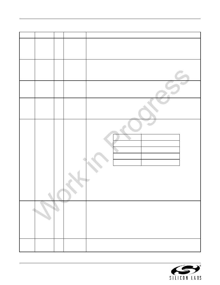
Table 6. Si5365 Pin Descriptions (Continued)
Pin #
Pin Name
I/O Signal Level
Description
CS[1:0]
Active Input Clock
00
CKIN1
01
CKIN2
10
CKIN3
11
CKIN4
相关PDF资料 |
PDF描述 |
|---|---|
| EMM11DSEH-S243 | CONN EDGECARD 22POS .156 EYELET |
| SI5322/23-EVB | BOARD EVAL FOR SI5322/23 |
| LBC2518T150K | INDUCTOR WOUND 15UH 285MA 1007 |
| GBM22DTBT-S189 | CONN EDGECARD 44POS R/A .156 SLD |
| 6754410-6 | CA,XG,MTRJ-SC |
相关代理商/技术参数 |
参数描述 |
|---|---|
| Si5365-B-GQ | 功能描述:时钟合成器/抖动清除器 PIN-PROGRAMMABLE CLK MULTIPLIER 5 OUTS RoHS:否 制造商:Skyworks Solutions, Inc. 输出端数量: 输出电平: 最大输出频率: 输入电平: 最大输入频率:6.1 GHz 电源电压-最大:3.3 V 电源电压-最小:2.7 V 封装 / 箱体:TSSOP-28 封装:Reel |
| SI5365-B-GQR | 制造商:Silicon Laboratories Inc 功能描述: |
| Si5365-C-GQ | 功能描述:时钟合成器/抖动清除器 PIN-PROGRAMMABLE CLK MULTIPLIER 5 OUTS RoHS:否 制造商:Skyworks Solutions, Inc. 输出端数量: 输出电平: 最大输出频率: 输入电平: 最大输入频率:6.1 GHz 电源电压-最大:3.3 V 电源电压-最小:2.7 V 封装 / 箱体:TSSOP-28 封装:Reel |
| SI5365-C-GQR | 功能描述:时钟发生器及支持产品 Pin-Progrm Precision Clk Xplier 4In/5Out RoHS:否 制造商:Silicon Labs 类型:Clock Generators 最大输入频率:14.318 MHz 最大输出频率:166 MHz 输出端数量:16 占空比 - 最大:55 % 工作电源电压:3.3 V 工作电源电流:1 mA 最大工作温度:+ 85 C 安装风格:SMD/SMT 封装 / 箱体:QFN-56 |
| SI5365-EVB | 制造商:Silicon Laboratories Inc 功能描述: |
发布紧急采购,3分钟左右您将得到回复。