- 您现在的位置:买卖IC网 > PDF目录4041 > MPC8568VTAUJJ (Freescale Semiconductor)MPU POWERQUICC III 1023-PBGA PDF资料下载
参数资料
| 型号: | MPC8568VTAUJJ |
| 厂商: | Freescale Semiconductor |
| 文件页数: | 72/139页 |
| 文件大小: | 0K |
| 描述: | MPU POWERQUICC III 1023-PBGA |
| 标准包装: | 24 |
| 系列: | MPC85xx |
| 处理器类型: | 32-位 MPC85xx PowerQUICC III |
| 速度: | 1.333GHz |
| 电压: | 1.1V |
| 安装类型: | 表面贴装 |
| 封装/外壳: | 1023-BBGA,FCBGA |
| 供应商设备封装: | 1023-FCPBGA(33x33) |
| 包装: | 托盘 |
第1页第2页第3页第4页第5页第6页第7页第8页第9页第10页第11页第12页第13页第14页第15页第16页第17页第18页第19页第20页第21页第22页第23页第24页第25页第26页第27页第28页第29页第30页第31页第32页第33页第34页第35页第36页第37页第38页第39页第40页第41页第42页第43页第44页第45页第46页第47页第48页第49页第50页第51页第52页第53页第54页第55页第56页第57页第58页第59页第60页第61页第62页第63页第64页第65页第66页第67页第68页第69页第70页第71页当前第72页第73页第74页第75页第76页第77页第78页第79页第80页第81页第82页第83页第84页第85页第86页第87页第88页第89页第90页第91页第92页第93页第94页第95页第96页第97页第98页第99页第100页第101页第102页第103页第104页第105页第106页第107页第108页第109页第110页第111页第112页第113页第114页第115页第116页第117页第118页第119页第120页第121页第122页第123页第124页第125页第126页第127页第128页第129页第130页第131页第132页第133页第134页第135页第136页第137页第138页第139页
MPC8568E/MPC8567E PowerQUICC III Integrated Processor Hardware Specifications, Rev. 1
38
Freescale Semiconductor
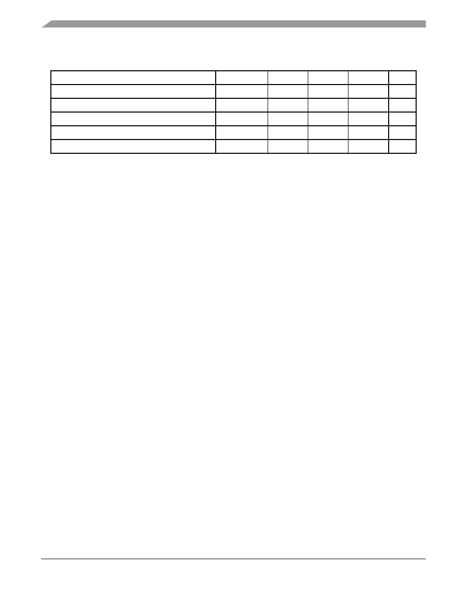
Ethernet Interface and MII Management
Duty cycle for 10BASE-T and 100BASE-TX 3, 4
tRGTH/tRGT
5
40
50
60
%
Rise time (20%–80%)
tRGTR
5
—0.75
1.5
ns
Fall time (20%–80%)
tRGTF
5
—0.75
1.5
ns
EC_GTX_CLK125 clock rise time (20%-80%)
tG125R
—0.75
1.5
ns
EC_GTX_CLK125 clock fall time (80%-20%)
tG125F
—0.75
1.5
ns
EC_GTX_CLK125 duty cycle6
tG125H/tG125
47
53
ns
Notes:
1. Note that, in general, the clock reference symbol representation for this section is based on the symbols RGT to
represent RGMII and RTBI timing. For example, the subscript of tRGT represents the TBI (T) receive (RX) clock. Note
also that the notation for rise (R) and fall (F) times follows the clock symbol that is being represented. For symbols
representing skews, the subscript is skew (SK) followed by the clock that is being skewed (RGT).
2. This implies that PC board design will require clocks to be routed such that an additional trace delay of greater than
1.5 ns will be added to the associated clock signal.
3. For 10 and 100 Mbps, tRGT scales to 400 ns ± 40 ns and 40 ns ± 4 ns, respectively.
4. Duty cycle may be stretched/shrunk during speed changes or while transitioning to a received packet's clock domains
as long as the minimum duty cycle is not violated and stretching occurs for no more than three tRGT of the lowest speed
transitioned between.
5. Guaranteed by characterization
6. EC_GTX_CLK125 is used to generate GTX_CLK for the eTSEC transmitter with 2% degradation. EC_GTX_CLK125
duty cycle can be loosen from 47/53% as long as the PHY device can tolerate the duty cycle generated by the eTSEC
GTX_CLK.
Table 34. RGMII and RTBI AC Timing Specifications (continued)
At recommended operating conditions with LVDD of 2.5 V ± 5%.
相关PDF资料 |
PDF描述 |
|---|---|
| MPC8547EVTATGB | MPU POWERQUICC III 783-PBGA |
| IDT71T75802S166PFGI8 | IC SRAM 18MBIT 166MHZ 100TQFP |
| AMC17DTEH | CONN EDGECARD 34POS .100 EYELET |
| FMC40DRYI-S13 | CONN EDGECARD 80POS .100 EXTEND |
| ABB105DHBN | CONN EDGECARD 210PS R/A .050 SLD |
相关代理商/技术参数 |
参数描述 |
|---|---|
| MPC8569CVTANKGB | 功能描述:数字信号处理器和控制器 - DSP, DSC 8569 XT 800/600/400 r2.1 RoHS:否 制造商:Microchip Technology 核心:dsPIC 数据总线宽度:16 bit 程序存储器大小:16 KB 数据 RAM 大小:2 KB 最大时钟频率:40 MHz 可编程输入/输出端数量:35 定时器数量:3 设备每秒兆指令数:50 MIPs 工作电源电压:3.3 V 最大工作温度:+ 85 C 封装 / 箱体:TQFP-44 安装风格:SMD/SMT |
| MPC8569CVTAQLJB | 功能描述:数字信号处理器和控制器 - DSP, DSC 8569 XT 1067/667/533 r2.1 RoHS:否 制造商:Microchip Technology 核心:dsPIC 数据总线宽度:16 bit 程序存储器大小:16 KB 数据 RAM 大小:2 KB 最大时钟频率:40 MHz 可编程输入/输出端数量:35 定时器数量:3 设备每秒兆指令数:50 MIPs 工作电源电压:3.3 V 最大工作温度:+ 85 C 封装 / 箱体:TQFP-44 安装风格:SMD/SMT |
| MPC8569ECVTANKGB | 功能描述:数字信号处理器和控制器 - DSP, DSC 8569E XT 800/600/400 r2.1 RoHS:否 制造商:Microchip Technology 核心:dsPIC 数据总线宽度:16 bit 程序存储器大小:16 KB 数据 RAM 大小:2 KB 最大时钟频率:40 MHz 可编程输入/输出端数量:35 定时器数量:3 设备每秒兆指令数:50 MIPs 工作电源电压:3.3 V 最大工作温度:+ 85 C 封装 / 箱体:TQFP-44 安装风格:SMD/SMT |
| MPC8569ECVTAQLJB | 功能描述:数字信号处理器和控制器 - DSP, DSC 8569E XT1067/667/533 r2.1 RoHS:否 制造商:Microchip Technology 核心:dsPIC 数据总线宽度:16 bit 程序存储器大小:16 KB 数据 RAM 大小:2 KB 最大时钟频率:40 MHz 可编程输入/输出端数量:35 定时器数量:3 设备每秒兆指令数:50 MIPs 工作电源电压:3.3 V 最大工作温度:+ 85 C 封装 / 箱体:TQFP-44 安装风格:SMD/SMT |
| MPC8569E-MDS-PB | 功能描述:开发板和工具包 - 其他处理器 MPC8569 MDS PROCESSOR BD RoHS:否 制造商:Freescale Semiconductor 产品:Development Systems 工具用于评估:P3041 核心:e500mc 接口类型:I2C, SPI, USB 工作电源电压: |
发布紧急采购,3分钟左右您将得到回复。