- 您现在的位置:买卖IC网 > PDF目录16490 > AD6641-500EBZ (Analog Devices Inc)BOARD EVALUATION FOR AD6641 PDF资料下载
参数资料
| 型号: | AD6641-500EBZ |
| 厂商: | Analog Devices Inc |
| 文件页数: | 17/28页 |
| 文件大小: | 0K |
| 描述: | BOARD EVALUATION FOR AD6641 |
| 设计资源: | AD6641 BOM |
| 标准包装: | 1 |
| 系列: | * |
第1页第2页第3页第4页第5页第6页第7页第8页第9页第10页第11页第12页第13页第14页第15页第16页当前第17页第18页第19页第20页第21页第22页第23页第24页第25页第26页第27页第28页
AD6641
Rev. 0 | Page 24 of 28
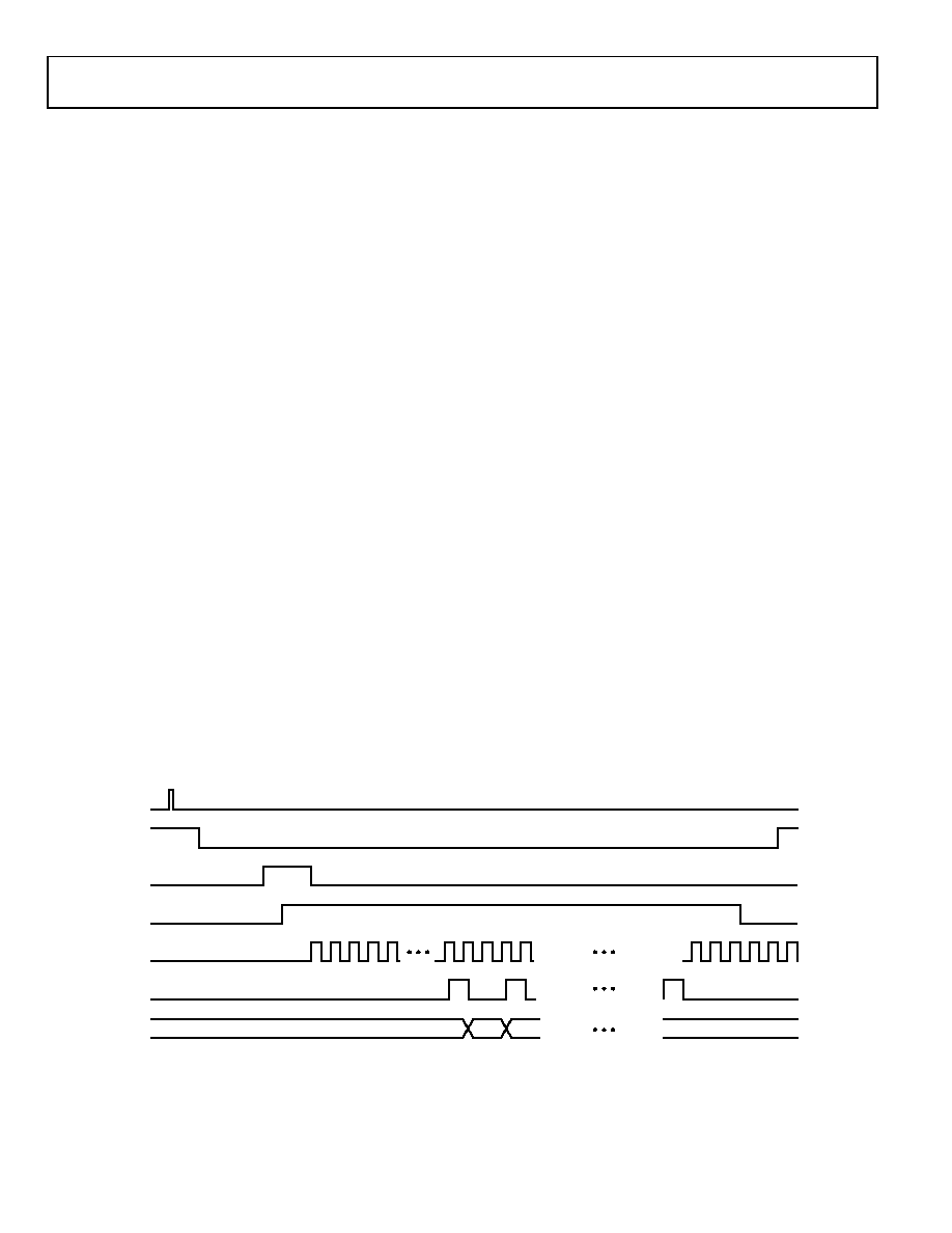
SPORT Master Mode (Single Capture)
Details of the transaction diagram for serial master mode are
shown in Figure 39 for single capture mode with the SDO
output. Clock cycles are approximate because the fill and dump
signals can be driven asynchronously. In this example, SCLK is
derived from the master clock with a divide by 8 programmed
from the SPI.
Fill Pulse (1)
The FIFO captures data after a fill signal (high level) is detected
on the rising edge of the sampling clock. In synchronous opera-
tion, a valid high level is accomplished by adhering to the setup
and hold times specified. For nonsynchronous control, the fill
signal can be widened to accommodate two or more clock
cycles to guarantee capture of a high level. Fill count (0x104) is
reset on the rising edge of the clock and is incremented on
subsequent clock cycles only after the fill signal returns low.
A new fill signal at any point during the capture resets the
counter and begins filling the FIFO.
Empty Signal (2)
After the FIFO state machine has begun loading data, the empty
signal goes low 24 clock cycles after the fill signal was last
sampled high.
Full Signal (3)
The full signal indicates when the FIFO has been filled and is
driven high when the number of samples specified has been
captured in the FIFO, where
Number of Samples = (FILL_CNT + 1) × 64
The time at which the full signal goes high is based on
(FILL_CNT + 1) × 64 + 13 clock cycles after the fill signal was
last sampled high.
Dump Signal (4)—Transition to High
The dump signal initiates reading data from the FIFO. Dump is
enabled with a high level and should be initiated only after the
full signal goes high. The dump signal should be held high until
all data has been read out of the FIFO.
SCLK Signal (5)
The SCLK (serial clock) signal is configured as an output from
the device when in the master mode of operation. SCLK begins
cycling five ADC clock cycles after the dump signal is sampled
high and continues cycling up until one additional cycle after
the empty signal goes high. SCLK then remains low until the
next dump operation.
SDFS Signal (6)
The SDFS (serial data frame sync) signal is configured as an
output from the device when in the master mode of operation.
Frame synchronization begins 15 ADC clock cycles after the
dump signal is sampled.
Dump Signal (7)—Transition to Low
A dump signal transition to low is applied after data has been
read out of the FIFO.
Empty Signal (8)—Transition to High
The empty signal transitions to high after data has been output
from the FIFO based on the clock cycle count of (FILL_CNT +
1) × 64.
The transition occurs 76 ADC clock cycles after the last LSB(s)
of data have been output on the serial port.
FILL
1
2
3
4
5
6
7
8
EMPTY
FULL
DUMP
SCLK
SDFS
SDO
09
81
3-0
37
Figure 39. SPORT Master Mode Transaction Diagram
相关PDF资料 |
PDF描述 |
|---|---|
| EBM30DTBD | CONN EDGECARD 60POS R/A .156 SLD |
| HCC07DRTH-S93 | CONN EDGECARD 14POS DIP .100 SLD |
| 1906051-8 | CA 2MM OFNR 62.5/125,LC SEC RED |
| 1828875-2 | C/A FO LC SEC SC BLUE 62.5 2M |
| A3932SEQ-T | IC CTRLR MOSFET 3PH 32-PLCC |
相关代理商/技术参数 |
参数描述 |
|---|---|
| AD6641BCPZ-500 | 功能描述:IC IF RCVR 11BIT 200MSPS 56LFCSP RoHS:是 类别:集成电路 (IC) >> 接口 - 专用 系列:- 特色产品:NXP - I2C Interface 标准包装:1 系列:- 应用:2 通道 I²C 多路复用器 接口:I²C,SM 总线 电源电压:2.3 V ~ 5.5 V 封装/外壳:16-TSSOP(0.173",4.40mm 宽) 供应商设备封装:16-TSSOP 包装:剪切带 (CT) 安装类型:表面贴装 产品目录页面:825 (CN2011-ZH PDF) 其它名称:568-1854-1 |
| AD6641BCPZRL7-500 | 功能描述:IC IF RCVR 11BIT 200MSPS 56LFCSP RoHS:是 类别:集成电路 (IC) >> 接口 - 专用 系列:- 特色产品:NXP - I2C Interface 标准包装:1 系列:- 应用:2 通道 I²C 多路复用器 接口:I²C,SM 总线 电源电压:2.3 V ~ 5.5 V 封装/外壳:16-TSSOP(0.173",4.40mm 宽) 供应商设备封装:16-TSSOP 包装:剪切带 (CT) 安装类型:表面贴装 产品目录页面:825 (CN2011-ZH PDF) 其它名称:568-1854-1 |
| AD6642 | 制造商:AD 制造商全称:Analog Devices 功能描述:Dual IF Receiver |
| AD6642BBCZ | 功能描述:IC IF RCVR 11BIT 200MSPS 144BGA RoHS:是 类别:RF/IF 和 RFID >> RF 其它 IC 和模块 系列:- 标准包装:100 系列:* |
| AD6642BBCZRL | 功能描述:IC IF RCVR 11BIT 200MSPS 144BGA RoHS:是 类别:RF/IF 和 RFID >> RF 其它 IC 和模块 系列:- 标准包装:100 系列:* |
发布紧急采购,3分钟左右您将得到回复。