- 您现在的位置:买卖IC网 > PDF目录4051 > MC8610VT800GB (Freescale Semiconductor)MPU E600 CORE 800MHZ 783-PBGA PDF资料下载
参数资料
| 型号: | MC8610VT800GB |
| 厂商: | Freescale Semiconductor |
| 文件页数: | 38/96页 |
| 文件大小: | 0K |
| 描述: | MPU E600 CORE 800MHZ 783-PBGA |
| 标准包装: | 36 |
| 系列: | MPC86xx |
| 处理器类型: | 32-位 MPC86xx PowerPC |
| 速度: | 800MHz |
| 电压: | 1V |
| 安装类型: | 表面贴装 |
| 封装/外壳: | 783-BBGA,FCBGA |
| 供应商设备封装: | 783-FCPBGA(29x29) |
| 包装: | 托盘 |
第1页第2页第3页第4页第5页第6页第7页第8页第9页第10页第11页第12页第13页第14页第15页第16页第17页第18页第19页第20页第21页第22页第23页第24页第25页第26页第27页第28页第29页第30页第31页第32页第33页第34页第35页第36页第37页当前第38页第39页第40页第41页第42页第43页第44页第45页第46页第47页第48页第49页第50页第51页第52页第53页第54页第55页第56页第57页第58页第59页第60页第61页第62页第63页第64页第65页第66页第67页第68页第69页第70页第71页第72页第73页第74页第75页第76页第77页第78页第79页第80页第81页第82页第83页第84页第85页第86页第87页第88页第89页第90页第91页第92页第93页第94页第95页第96页
Electrical Characteristics
MPC8610 Integrated Host Processor Hardware Specifications, Rev. 2
Freescale Semiconductor
43
2.12.2
SSI AC Timing Specifications
All timings for the SSI are given for a noninverted serial clock polarity (TSCKP/RSCKP = 0) and a noninverted frame sync
(TFSI/RFSI = 0). If the polarity of the clock and/or the frame sync have been inverted, all the timing remains valid by inverting
the clock signal STCK/SRCK and/or the frame sync STFS/SRFS shown in the following tables and figures.
For internal frame sync operation using external clock, the FS timing will be same as that of Tx Data.
2.12.2.1
SSI Transmitter Timing with Internal Clock
Table 35 provides the transmitter timing parameters with internal clock.
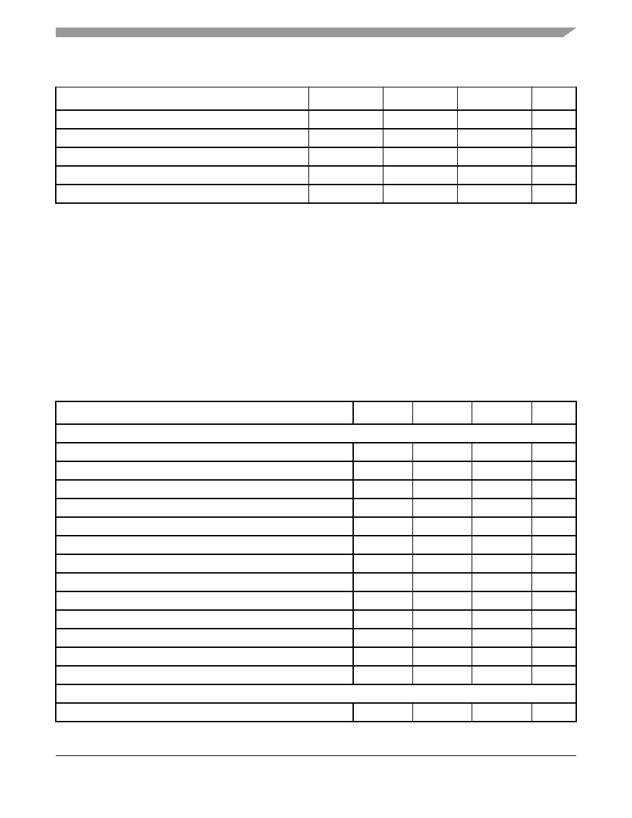
Table 34. SSI DC Electrical Characteristics (3.3 V DC)
Parameter
Symbol
Min
Max
Unit
High-level input voltage
VIH
2BVDD + 0.3
V
Low-level input voltage
VIL
–0.3
0.8
V
Input current (BVIN
1 = 0 V or BV
IN = BVDD)IIN
—±5
μA
High-level output voltage (BVDD = min, IOH = –2 mA)
VOH
BVDD – 0.2
—
V
Low-level output voltage (BVDD = min, IOL = 2 mA)
VOL
—0.2
V
Note:
Table 35. SSI Transmitter with Internal Clock Timing Parameters
Parameter
Symbol
Min
Max
Unit
Internal Clock Operation
(Tx/Rx) CK clock period
SS1
81.4
—
ns
(Tx/Rx) CK clock high period
SS2
36.0
—
ns
(Tx/Rx) CK clock rise time
SS3
—
6
ns
(Tx/Rx) CK clock low period
SS4
36.0
—
ns
(Tx/Rx) CK clock fall time
SS5
—
6
ns
(Tx) CK high to FS high
SS10
—
15.0
ns
(Tx) CK high to FS low
SS12
—
15.0
ns
(Tx/Rx) internal FS rise time
SS14
—
6
ns
(Tx/Rx) internal FS fall time
SS15
—
6
ns
(Tx) CK high to STXD valid from high impedance
SS16
—
15.0
ns
(Tx) CK high to STXD high/low
SS17
—
15.0
ns
(Tx) CK high to STXD high impedance
SS18
—
15.0
ns
STXD rise/fall time
SS19
—
6
ns
Synchronous Internal Clock Operation
SRXD setup before (Tx) CK falling
SS42
10.0
—
ns
相关PDF资料 |
PDF描述 |
|---|---|
| MPC8536CVTANGA | MPU POWERQUICC III 783FCPBGA |
| MPC755CVT350LE | MCU HIP4DP 350MHZ 360-PBGA |
| MPC755CRX350LE | MCU HIP4DP 350MHZ 360-CBGA |
| MPC755CPX350LE | MCU HIP4DP 350MHZ 360-PBGA |
| MPC755BVT350LE | MCU HIP4DP 350MHZ 360-PBGA |
相关代理商/技术参数 |
参数描述 |
|---|---|
| MC8610VT800GZ | 制造商:FREESCALE 制造商全称:Freescale Semiconductor, Inc 功能描述:MPC8610 Integrated Host Processor Hardware Specifications |
| MC8610VT800J | 制造商:FREESCALE 制造商全称:Freescale Semiconductor, Inc 功能描述:Integrated Host Processor Hardware Specifications |
| MC861P | 制造商:Motorola Inc 功能描述: 制造商:Texas Instruments 功能描述: |
| MC862 | 制造商:FREESCALE 制造商全称:Freescale Semiconductor, Inc 功能描述:INTEGRATED CIRCUITS |
| MC862L | 制造商:Motorola Inc 功能描述: |
发布紧急采购,3分钟左右您将得到回复。