- 您现在的位置:买卖IC网 > PDF目录17117 > DK-DEV-4SGX230N (Altera)KIT DEVELOPMENT STRATIX IV PDF资料下载
参数资料
| 型号: | DK-DEV-4SGX230N |
| 厂商: | Altera |
| 文件页数: | 69/82页 |
| 文件大小: | 0K |
| 描述: | KIT DEVELOPMENT STRATIX IV |
| 产品培训模块: | Three Reasons to Use FPGA's in Industrial Designs |
| 特色产品: | Stratix? IV GX FPGA Development Kit |
| 标准包装: | 1 |
| 系列: | Stratix® IV GX |
| 类型: | FPGA |
| 适用于相关产品: | EP4SGX230K |
| 所含物品: | 开发板、通用电源、缆线和软件 |
| 产品目录页面: | 607 (CN2011-ZH PDF) |
| 相关产品: | EP4SGX230KF40C3N-ND - IC STRATIX IV FPGA 230K 1517FBGA EP4SGX230KF40C3-ND - IC STRATIX IV FPGA 230K 1517FBGA EP4SGX230HF35C3N-ND - IC STRATIX IV GX 230K 1152-FBGA EP4SGX230HF35C3-ND - IC STRATIX IV GX 230K 1152-FBGA EP4SGX230FF35C3NES-ND - IC STRATIX IV GX 230K 1152-FBGA EP4SGX230FF35C3ES-ND - IC STRATIX IV GX 230K 1152-FBGA EP4SGX230DF29C3NES-ND - IC STRATIX IV GX 230K 780-FBGA EP4SGX230DF29C3ES-ND - IC STRATIX IV GX 230K 780-FBGA |
| 其它名称: | 544-2594 |
第1页第2页第3页第4页第5页第6页第7页第8页第9页第10页第11页第12页第13页第14页第15页第16页第17页第18页第19页第20页第21页第22页第23页第24页第25页第26页第27页第28页第29页第30页第31页第32页第33页第34页第35页第36页第37页第38页第39页第40页第41页第42页第43页第44页第45页第46页第47页第48页第49页第50页第51页第52页第53页第54页第55页第56页第57页第58页第59页第60页第61页第62页第63页第64页第65页第66页第67页第68页当前第69页第70页第71页第72页第73页第74页第75页第76页第77页第78页第79页第80页第81页第82页
Chapter 1: DC and Switching Characteristics for Stratix IV Devices
1–63
I/O Timing
March 2014
Altera Corporation
Stratix IV Device Handbook
Volume 4: Device Datasheet and Addendum
Programmable IOE Delay
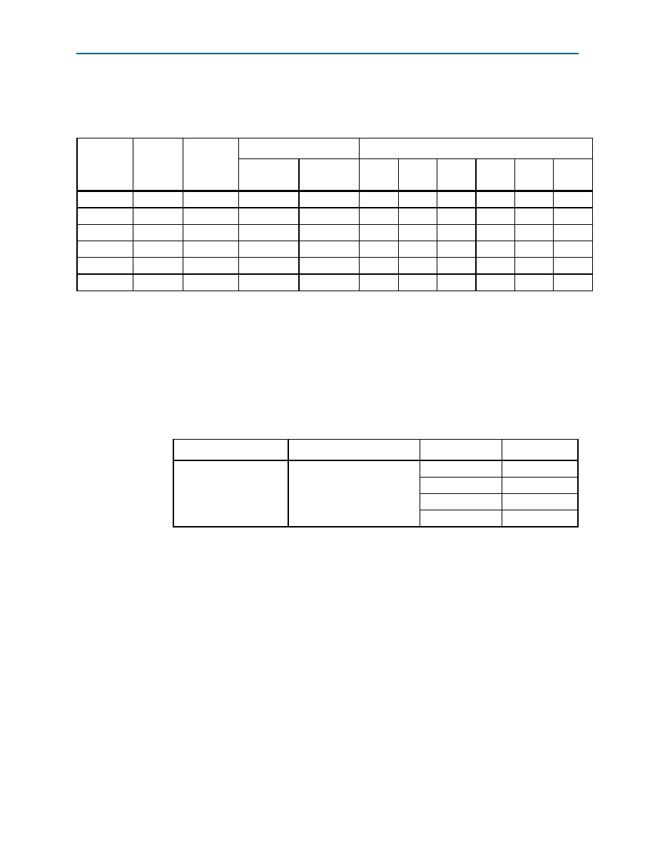
Table 1–52 lists the Stratix IV IOE programmable delay settings.
Programmable Output Buffer Delay
Table 1–53 lists the delay chain settings that control the rising and falling edge delays
of the output buffer. The default delay is 0 ps.
Table 1–52. IOE Programmable Delay for Stratix IV Devices
Parameter
Available
Settings
Min Offset
Fast Model
Slow Model
Industrial/
Military
Commercial
C2 (3)
C3
C4
I3/M3
I4
Unit
D1
16
0
0.462
0.505
0.732
0.795
0.857
0.801
0.864
ns
D2
8
0
0.234
0.232
0.337
0.372
0.407
0.371
0.405
ns
D3
8
0
1.700
1.769
2.695
2.927
3.157
2.948
3.178
ns
D4
16
0
0.508
0.554
0.813
0.882
0.952
0.889
0.959
ns
D5
16
0
0.472
0.500
0.747
0.799
0.875
0.817
0.882
ns
D6
7
0
0.186
0.195
0.294
0.319
0.345
0.321
0.347
ns
Notes to Table 1–52:
(1) You can set this value in the Quartus II software by selecting D1, D2, D3, D4, D5, and D6 in the Assignment Name column.
(2) Minimum offset does not include the intrinsic delay.
(3) For the EP4SGX530 device density, the IOE programmable delays have an additional 5% maximum offset.
Table 1–53. Programmable Output Buffer Delay (1)
Symbol
Parameter
Typical
Unit
DOUTBUF
Rising and/or falling edge
delay
0 (default)
ps
50
ps
100
ps
150
ps
Note to Table 1–53:
(1) You can set the programmable output buffer delay in the Quartus II software by setting the Output Buffer Delay
Control assignment to either positive, negative, or both edges, with the specific values stated here (in ps) for the
Output Buffer Delay assignment.
相关PDF资料 |
PDF描述 |
|---|---|
| VE-JTL-EZ | CONVERTER MOD DC/DC 28V 25W |
| VE-JTJ-EZ | CONVERTER MOD DC/DC 36V 25W |
| AP432L-13 | IC VREF SHUNT PREC ADJ 8-SOP |
| VE-JTH-EZ | CONVERTER MOD DC/DC 52V 25W |
| RW2-4812S/H3/SMD | CONV DC/DC 2W 36-72VIN 12VOUT |
相关代理商/技术参数 |
参数描述 |
|---|---|
| DK-DEV-4SGX230N/C2 | 功能描述:EP4SGX230KF40C2N Stratix? IV GX FPGA Evaluation Board 制造商:altera 系列:Stratix? IV GX 零件状态:过期 类型:FPGA 配套使用产品/相关产品:EP4SGX230KF40C2N 内容:板,线缆,电源 标准包装:1 |
| DK-DEV-4SGX530N | 功能描述:可编程逻辑 IC 开发工具 FPGA Development Kit For EP4SGX530 RoHS:否 制造商:Altera Corporation 产品:Development Kits 类型:FPGA 工具用于评估:5CEFA7F3 接口类型: 工作电源电压: |
| DK-DEV-5AGTD7N | 功能描述:可编程逻辑 IC 开发工具 FPGA Development Kit For 5AGTD7K3F40I3N RoHS:否 制造商:Altera Corporation 产品:Development Kits 类型:FPGA 工具用于评估:5CEFA7F3 接口类型: 工作电源电压: |
| DK-DEV-5AGXB3N/ES | 功能描述:可编程逻辑 IC 开发工具 FPGA Development Kit For 5AGXFB3H6F ES RoHS:否 制造商:Altera Corporation 产品:Development Kits 类型:FPGA 工具用于评估:5CEFA7F3 接口类型: 工作电源电压: |
| DK-DEV-5ASTD5N | 功能描述:KIT DEV ARRIA V FPGA 制造商:altera 系列:Arria V ST 零件状态:在售 类型:FPGA 配套使用产品/相关产品:Arria? V ST 内容:板 标准包装:1 |
发布紧急采购,3分钟左右您将得到回复。