- 您现在的位置:买卖IC网 > PDF目录17117 > DK-DEV-4SGX230N (Altera)KIT DEVELOPMENT STRATIX IV PDF资料下载
参数资料
| 型号: | DK-DEV-4SGX230N |
| 厂商: | Altera |
| 文件页数: | 10/82页 |
| 文件大小: | 0K |
| 描述: | KIT DEVELOPMENT STRATIX IV |
| 产品培训模块: | Three Reasons to Use FPGA's in Industrial Designs |
| 特色产品: | Stratix? IV GX FPGA Development Kit |
| 标准包装: | 1 |
| 系列: | Stratix® IV GX |
| 类型: | FPGA |
| 适用于相关产品: | EP4SGX230K |
| 所含物品: | 开发板、通用电源、缆线和软件 |
| 产品目录页面: | 607 (CN2011-ZH PDF) |
| 相关产品: | EP4SGX230KF40C3N-ND - IC STRATIX IV FPGA 230K 1517FBGA EP4SGX230KF40C3-ND - IC STRATIX IV FPGA 230K 1517FBGA EP4SGX230HF35C3N-ND - IC STRATIX IV GX 230K 1152-FBGA EP4SGX230HF35C3-ND - IC STRATIX IV GX 230K 1152-FBGA EP4SGX230FF35C3NES-ND - IC STRATIX IV GX 230K 1152-FBGA EP4SGX230FF35C3ES-ND - IC STRATIX IV GX 230K 1152-FBGA EP4SGX230DF29C3NES-ND - IC STRATIX IV GX 230K 780-FBGA EP4SGX230DF29C3ES-ND - IC STRATIX IV GX 230K 780-FBGA |
| 其它名称: | 544-2594 |
第1页第2页第3页第4页第5页第6页第7页第8页第9页当前第10页第11页第12页第13页第14页第15页第16页第17页第18页第19页第20页第21页第22页第23页第24页第25页第26页第27页第28页第29页第30页第31页第32页第33页第34页第35页第36页第37页第38页第39页第40页第41页第42页第43页第44页第45页第46页第47页第48页第49页第50页第51页第52页第53页第54页第55页第56页第57页第58页第59页第60页第61页第62页第63页第64页第65页第66页第67页第68页第69页第70页第71页第72页第73页第74页第75页第76页第77页第78页第79页第80页第81页第82页
Chapter 1: DC and Switching Characteristics for Stratix IV Devices
1–10
Electrical Characteristics
March 2014
Altera Corporation
Stratix IV Device Handbook
Volume 4: Device Datasheet and Addendum
OCT calibration is automatically performed at power-up for OCT-enabled I/Os.
Table 1–13 lists OCT variation with temperature and voltage after power-up
calibration. Use Table 1–13 to determine the OCT variation after power-up calibration
and Equation 1–1 to determine the OCT variation without re-calibration.
Table 1–13 lists the OCT variation after the power-up calibration.
Pin Capacitance
Table 1–14 lists the Stratix IV device family pin capacitance.
Notes to Equation 1–1:
(1) The ROCT value calculated from Equation 1–1 shows the range of OCT resistance with the variation of temperature
and VCCIO.
(2) RSCAL is the OCT resistance value at power-up.
(3)
T is the variation of temperature with respect to the temperature at power-up.
(4)
V is the variation of voltage with respect to the V
CCIO at power-up.
(5) dR/dT is the percentage change of RSCAL with temperature.
(6) dR/dV is the percentage change of RSCAL with voltage.
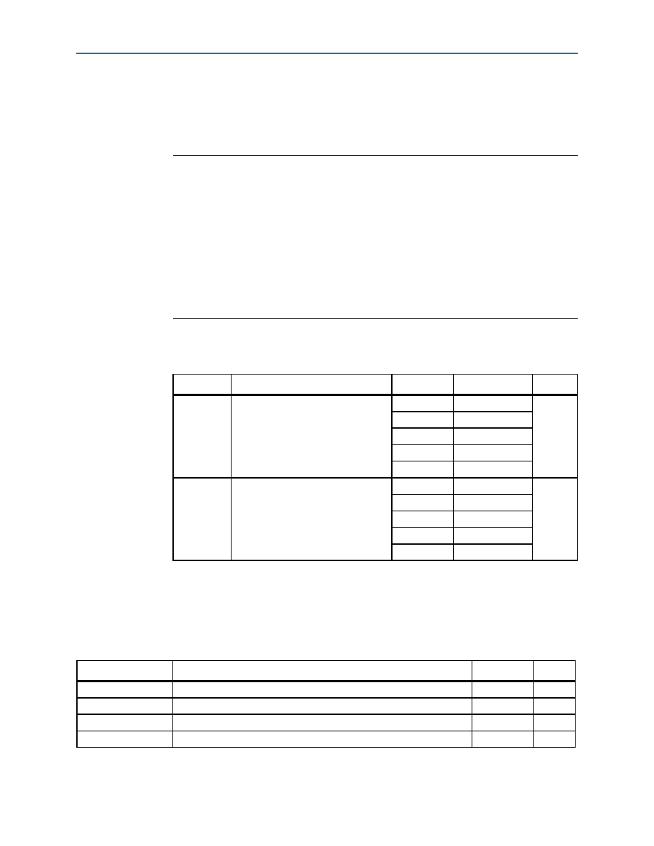
Table 1–13. OCT Variation after Power-Up Calibration (1)
Symbol
Description
VCCIO (V)
Typical
Unit
dR/dV
OCT variation with voltage without
re-calibration
3.0
0.0297
%/mV
2.5
0.0344
1.8
0.0499
1.5
0.0744
1.2
0.1241
dR/dT
OCT variation with temperature
without re-calibration
3.0
0.189
%/°C
2.5
0.208
1.8
0.266
1.5
0.273
1.2
0.317
Note to Table 1–13:
(1) Valid for VCCIO range of ±5% and temperature range of 0° to 85°C.
ROCT
RSCAL 1
dR
dT
-------
T
dR
dV
-------
V
+
=
Table 1–14. Pin Capacitance for Stratix IV Devices (Part 1 of 2)
Symbol
Description
Value
Unit
CIOTB
Input capacitance on the top and bottom I/O pins
4
pF
CIOLR
Input capacitance on the left and right I/O pins
4
pF
CCLKTB
Input capacitance on the top and bottom non-dedicated clock input pins
4
pF
CCLKLR
Input capacitance on the left and right non-dedicated clock input pins
4
pF
相关PDF资料 |
PDF描述 |
|---|---|
| VE-JTL-EZ | CONVERTER MOD DC/DC 28V 25W |
| VE-JTJ-EZ | CONVERTER MOD DC/DC 36V 25W |
| AP432L-13 | IC VREF SHUNT PREC ADJ 8-SOP |
| VE-JTH-EZ | CONVERTER MOD DC/DC 52V 25W |
| RW2-4812S/H3/SMD | CONV DC/DC 2W 36-72VIN 12VOUT |
相关代理商/技术参数 |
参数描述 |
|---|---|
| DK-DEV-4SGX230N/C2 | 功能描述:EP4SGX230KF40C2N Stratix? IV GX FPGA Evaluation Board 制造商:altera 系列:Stratix? IV GX 零件状态:过期 类型:FPGA 配套使用产品/相关产品:EP4SGX230KF40C2N 内容:板,线缆,电源 标准包装:1 |
| DK-DEV-4SGX530N | 功能描述:可编程逻辑 IC 开发工具 FPGA Development Kit For EP4SGX530 RoHS:否 制造商:Altera Corporation 产品:Development Kits 类型:FPGA 工具用于评估:5CEFA7F3 接口类型: 工作电源电压: |
| DK-DEV-5AGTD7N | 功能描述:可编程逻辑 IC 开发工具 FPGA Development Kit For 5AGTD7K3F40I3N RoHS:否 制造商:Altera Corporation 产品:Development Kits 类型:FPGA 工具用于评估:5CEFA7F3 接口类型: 工作电源电压: |
| DK-DEV-5AGXB3N/ES | 功能描述:可编程逻辑 IC 开发工具 FPGA Development Kit For 5AGXFB3H6F ES RoHS:否 制造商:Altera Corporation 产品:Development Kits 类型:FPGA 工具用于评估:5CEFA7F3 接口类型: 工作电源电压: |
| DK-DEV-5ASTD5N | 功能描述:KIT DEV ARRIA V FPGA 制造商:altera 系列:Arria V ST 零件状态:在售 类型:FPGA 配套使用产品/相关产品:Arria? V ST 内容:板 标准包装:1 |
发布紧急采购,3分钟左右您将得到回复。