参数资料
| 型号: | AD5749ACPZ |
| 厂商: | Analog Devices Inc |
| 文件页数: | 27/28页 |
| 文件大小: | 0K |
| 描述: | IC CURRENT OUT DVR 32-LFCSP |
| 标准包装: | 1 |
| 放大器类型: | 仪表 |
| 电路数: | 1 |
| 电流 - 电源: | 5.2mA |
| 电流 - 输出 / 通道: | 24mA |
| 电压 - 电源,单路/双路(±): | 10.8 V ~ 55 V |
| 工作温度: | -40°C ~ 105°C |
| 安装类型: | 表面贴装 |
| 封装/外壳: | 32-VFQFN 裸露焊盘,CSP |
| 供应商设备封装: | 32-LFCSP-VQ(5x5) |
| 包装: | 托盘 |
第1页第2页第3页第4页第5页第6页第7页第8页第9页第10页第11页第12页第13页第14页第15页第16页第17页第18页第19页第20页第21页第22页第23页第24页第25页第26页当前第27页第28页
AD5749
Data Sheet
Rev. B | Page 8 of 28
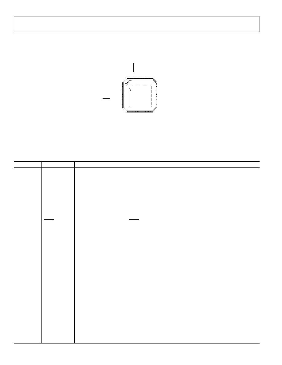
PIN CONFIGURATION AND FUNCTION DESCRIPTIONS
Figure 4. Pin Configuration
Table 5. Pin Function Descriptions
Pin No.
Mnemonic
Description
1
SDO/VFAULT
Serial Data Output (SDO). In software mode, this pin is used to clock data from the input shift register in
readback mode. Data is clocked out on the rising edge of SCLK and is valid on the falling edge of SCLK.
This pin is a CMOS output.
2
CLRSEL
In hardware or software mode, this pin selects the clear value, either zero scale or midscale. In software
mode, this pin is implemented as a logic OR with the internal CLRSEL bit.
3
CLEAR
Active High Input. Asserting this pin sets the output current to zero-scale code or midscale of range
selected (user selectable). CLEAR is a logic OR with the internal CLEAR bit. See the Asynchronous Clear
(CLEAR) section for more details.
4
DVCC
Digital Power Supply.
5
GND
Ground Connection.
6
SYNC/RSET
Positive Edge-Sensitive Latch (SYNC). In software mode, a rising edge parallel loads the input shift
register data into the AD5749 and also updates the output.
Resistor Select (RSET). In hardware mode, this pin selects whether the internal or the external current
sense resistor is used.
If RSET = 0, the external sense resistor is chosen.
If RSET = 1, the internal sense resistor is chosen.
7
SCLK/OUTEN
Serial Clock Input (SCLK). In software mode, data is clocked into the input shift register on the falling
edge of SCLK. This pin operates at clock speeds up to 50 MHz.
Output Enable (OUTEN). In hardware mode, this pin acts as an output enable pin.
8
SDIN/R0
Serial Data Input (SDIN). In software mode, data must be valid on the falling edge of SCLK.
Range Decode Bit (R0). In hardware mode, this pin, in conjunction with R1, R2, and R3, selects the output
current range setting on the part.
9
AD2/R1
Device Addressing Bit (AD2). In software mode, this pin, in conjunction with AD0 and AD1, allows up to
eight devices to be addressed on one bus.
Range Decode Bit (R1). In hardware mode, this pin, in conjunction with R0, R2, and R3, selects the output
current range setting on the part.
10
AD1/R2
Device Addressing Bit (AD1). In software mode, this pin, in conjunction with AD0 and AD2, allows up to
eight devices to be addressed on one bus.
Range Decode Bit (R2). In hardware mode, this pin, in conjunction with R0, R1, and R3, selects the output
current range setting on the part.
11
AD0/R3
Device Addressing Bit (AD0). In software mode, this pin, in conjunction with AD1 and AD2, allows up to
eight devices to be addressed on one bus.
Range Decode Bit (R3). In hardware mode, this pin, in conjunction with R0, R1, and R2, selects the output
current range setting on the part.
PIN 1
INDICATOR
TOP VIEW
(Not to Scale)
AD5749
1
SDO/VFAULT
2
CLRSEL
3
CLEAR
4
DVCC
5
GND
6
SYNC/RSET
7
SCLK/OUTEN
8
SDIN/R0
24 DNC
23 DNC
22 GND
21 GND
20 DNC
19 DNC
18 IOUT
17 AVDD
9
AD
2
/R
1
0
AD
1
/R
2
1
AD
0
/R
3
1
2
R
EX
T
2
1
3
R
EX
T
1
4
V
R
EF
1
5
V
IN
1
6
G
N
D
3
2
NC
/I
F
AU
L
T
3
1
F
AU
LT
/T
EMP
3
0
R
ESET
2
9
H
W
SE
L
E
C
T
2
8
N
C
2
7
N
C
2
6
N
C
2
5
N
C
08923-
004
NOTES
1. NC = NO CONNECT.
2. THE EXPOSED PADDLE IS TIED TO GND.
相关PDF资料 |
PDF描述 |
|---|---|
| AD5750-1ACPZ-REEL7 | IC CURR/VOLT OUT DVR 32LFCSP |
| AD5750-2BCPZ-RL7 | IC CURR/VOLT OUT DRVR 32LFCSP |
| AD5751ACPZ-REEL7 | IC I/V OUTPUT DRIVER 60V 32LFCSP |
| AD582SD | IC AMP SAMPLE HOLD 25MA 14CDIP |
| AD585SQ | IC AMP SAMPLE HOLD 50MA 14CDIP |
相关代理商/技术参数 |
参数描述 |
|---|---|
| AD5749ACPZ-RL7 | 功能描述:IC CURRENT OUT DVR 32-LFCSP RoHS:是 类别:集成电路 (IC) >> Linear - Amplifiers - Instrumentation 系列:- 标准包装:50 系列:LinCMOS™ 放大器类型:通用 电路数:4 输出类型:- 转换速率:0.05 V/µs 增益带宽积:110kHz -3db带宽:- 电流 - 输入偏压:0.7pA 电压 - 输入偏移:210µV 电流 - 电源:57µA 电流 - 输出 / 通道:30mA 电压 - 电源,单路/双路(±):3 V ~ 16 V,±1.5 V ~ 8 V 工作温度:-40°C ~ 85°C 安装类型:表面贴装 封装/外壳:14-SOIC(0.154",3.90mm 宽) 供应商设备封装:14-SOIC 包装:管件 产品目录页面:865 (CN2011-ZH PDF) 其它名称:296-1834296-1834-5 |
| AD574A | 制造商:AD 制造商全称:Analog Devices 功能描述:Complete 12-Bit A/D Converter |
| AD574AJ | 制造商:AD 制造商全称:Analog Devices 功能描述:Complete 12-Bit A/D Converter |
| AD574AJD | 功能描述:IC ADC 12BIT W/REF 28-CDIP RoHS:否 类别:集成电路 (IC) >> 数据采集 - 模数转换器 系列:- 标准包装:1 系列:- 位数:14 采样率(每秒):83k 数据接口:串行,并联 转换器数目:1 功率耗散(最大):95mW 电压电源:双 ± 工作温度:0°C ~ 70°C 安装类型:通孔 封装/外壳:28-DIP(0.600",15.24mm) 供应商设备封装:28-PDIP 包装:管件 输入数目和类型:1 个单端,双极 |
发布紧急采购,3分钟左右您将得到回复。