参数资料
| 型号: | XC6SLX45T-3FG484I |
| 厂商: | Xilinx Inc |
| 文件页数: | 58/89页 |
| 文件大小: | 0K |
| 描述: | IC FPGA SPARTAN 6 484FGGBGA |
| 标准包装: | 60 |
| 系列: | Spartan® 6 LXT |
| LAB/CLB数: | 3411 |
| 逻辑元件/单元数: | 43661 |
| RAM 位总计: | 2138112 |
| 输入/输出数: | 296 |
| 电源电压: | 1.14 V ~ 1.26 V |
| 安装类型: | 表面贴装 |
| 工作温度: | -40°C ~ 100°C |
| 封装/外壳: | 484-BBGA |
| 供应商设备封装: | 484-FBGA |
第1页第2页第3页第4页第5页第6页第7页第8页第9页第10页第11页第12页第13页第14页第15页第16页第17页第18页第19页第20页第21页第22页第23页第24页第25页第26页第27页第28页第29页第30页第31页第32页第33页第34页第35页第36页第37页第38页第39页第40页第41页第42页第43页第44页第45页第46页第47页第48页第49页第50页第51页第52页第53页第54页第55页第56页第57页当前第58页第59页第60页第61页第62页第63页第64页第65页第66页第67页第68页第69页第70页第71页第72页第73页第74页第75页第76页第77页第78页第79页第80页第81页第82页第83页第84页第85页第86页第87页第88页第89页
Spartan-6 FPGA Data Sheet: DC and Switching Characteristics
DS162 (v3.0) October 17, 2011
Product Specification
61
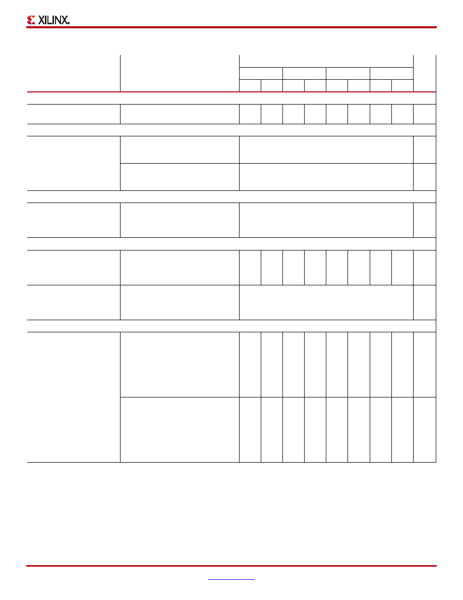
Table 56: Switching Characteristics for the Digital Frequency Synthesizer (DFS) for DCM_SP(1)
Symbol
Description
Speed Grade
Units
-3
-3N
-2
-1L
Min
Max
Min
Max
Min
Max
Min
Max
Output Frequency Ranges
CLKOUT_FREQ_FX
Frequency for the CLKFX and
CLKFX180 outputs
537553755333
5200
MHz
Output Clock Jitter(2)(3)
CLKOUT_PER_JITT_FX
Period jitter at the CLKFX and
CLKFX180 outputs. When
CLKIN < 20 MHz
Use the Clocking Wizard
ps
Period jitter at the CLKFX and
CLKFX180 outputs. When
CLKIN > 20 MHz
Typical = ±(1% of CLKFX period + 100)
ps
Duty Cycle(4)(5)
CLKOUT_DUTY_CYCLE_FX
Duty cycle precision for the CLKFX
and CLKFX180 outputs including the
BUFGMUX and clock tree duty-cycle
distortion
Maximum = ±(1% of CLKFX period + 350)
ps
Phase Alignment(5)
CLKOUT_PHASE_FX
Phase offset between the DFS
CLKFX output and the DLL CLK0
output when both the DFS and DLL
are used
–
±200
–
±200
–
±200
–
±250
ps
CLKOUT_PHASE_FX180
Phase offset between the DFS
CLKFX180 output and the DLL CLK0
output when both the DFS and DLL
are used
Maximum = ±(1% of CLKFX period + 200)
ps
LOCKED Time
LOCK_FX(2)
When FCLKIN < 50 MHz, the time
from deassertion at the DCM’s reset
input to the rising transition at its
LOCKED output. The DFS asserts
LOCKED when the CLKFX and
CLKFX180 signals are valid. When
using both the DLL and the DFS, use
the longer locking time.
–
5–5–5–
5
ms
When FCLKIN > 50 MHz, the time
from deassertion at the DCM’s reset
input to the rising transition at its
LOCKED output. The DFS asserts
LOCKED when the CLKFX and
CLKFX180 signals are valid. When
using both the DLL and the DFS, use
the longer locking time.
–0.45–0.45–0.45–
0.60
ms
Notes:
1.
2.
For optimal jitter tolerance and a faster LOCK time, use the CLKIN_PERIOD attribute.
3.
Output jitter is characterized with no input jitter. Output jitter strongly depends on the environment, including the number of SSOs, the output drive
strength, CLB utilization, CLB switching activities, switching frequency, power supply, and PCB design. The actual maximum output jitter depends on
the system application.
4.
The CLKFX, CLKFXDV, and CLKFX180 outputs have a duty cycle of approximately 50%.
5.
Some duty cycle and alignment specifications include a percentage of the CLKFX output period. For example, this data sheet specifies a maximum
CLKFX jitter of ±(1% of CLKFX period + 200 ps). Assuming that the CLKFX output frequency is 100 MHz, the equivalent CLKFX period is 10 ns, and
1% of 10 ns is 0.1 ns or 100 ps. Accordingly, the maximum jitter is ±(100 ps + 200 ps) = ±300 ps.
相关PDF资料 |
PDF描述 |
|---|---|
| ABB90DHFR | CONN EDGECARD 180POS .050 SMD |
| QLOCKPOST-5 | QUICK LOCK .067-.079" 4-40 KIT |
| 24FC128-I/MS | IC EEPROM 128KBIT 1MHZ 8MSOP |
| FSM28DSEN-S243 | CONN EDGECARD 56POS .156 EYELET |
| XA6SLX25T-2FGG484Q | IC FPGA SPARTAN 6 484FGGBGA |
相关代理商/技术参数 |
参数描述 |
|---|---|
| XC6SLX45T-3FGG484C | 功能描述:IC FPGA SPARTAN 6 43K 484FGGBGA RoHS:是 类别:集成电路 (IC) >> 嵌入式 - FPGA(现场可编程门阵列) 系列:Spartan® 6 LXT 标准包装:60 系列:XP LAB/CLB数:- 逻辑元件/单元数:10000 RAM 位总计:221184 输入/输出数:244 门数:- 电源电压:1.71 V ~ 3.465 V 安装类型:表面贴装 工作温度:0°C ~ 85°C 封装/外壳:388-BBGA 供应商设备封装:388-FPBGA(23x23) 其它名称:220-1241 |
| XC6SLX45T-3FGG484I | 功能描述:IC FPGA SPARTAN 6 43K 484FGGBGA RoHS:是 类别:集成电路 (IC) >> 嵌入式 - FPGA(现场可编程门阵列) 系列:Spartan® 6 LXT 产品变化通告:Step Intro and Pkg Change 11/March/2008 标准包装:1 系列:Virtex®-5 SXT LAB/CLB数:4080 逻辑元件/单元数:52224 RAM 位总计:4866048 输入/输出数:480 门数:- 电源电压:0.95 V ~ 1.05 V 安装类型:表面贴装 工作温度:-40°C ~ 100°C 封装/外壳:1136-BBGA,FCBGA 供应商设备封装:1136-FCBGA 配用:568-5088-ND - BOARD DEMO DAC1408D750122-1796-ND - EVALUATION PLATFORM VIRTEX-5 |
| XC6SLX45T-4CSG324C | 功能描述:IC FPGA SPARTAN 6 43K 324CSGBGA RoHS:是 类别:集成电路 (IC) >> 嵌入式 - FPGA(现场可编程门阵列) 系列:Spartan® 6 LXT 标准包装:1 系列:Kintex-7 LAB/CLB数:25475 逻辑元件/单元数:326080 RAM 位总计:16404480 输入/输出数:350 门数:- 电源电压:0.97 V ~ 1.03 V 安装类型:表面贴装 工作温度:0°C ~ 85°C 封装/外壳:900-BBGA,FCBGA 供应商设备封装:900-FCBGA(31x31) 其它名称:122-1789 |
| XC6SLX45T-4CSG484C | 功能描述:IC FPGA SPARTAN 6 43K 484CSGBGA RoHS:是 类别:集成电路 (IC) >> 嵌入式 - FPGA(现场可编程门阵列) 系列:Spartan® 6 LXT 标准包装:1 系列:Kintex-7 LAB/CLB数:25475 逻辑元件/单元数:326080 RAM 位总计:16404480 输入/输出数:350 门数:- 电源电压:0.97 V ~ 1.03 V 安装类型:表面贴装 工作温度:0°C ~ 85°C 封装/外壳:900-BBGA,FCBGA 供应商设备封装:900-FCBGA(31x31) 其它名称:122-1789 |
| XC6SLX45T-4FGG484C | 功能描述:IC FPGA SPARTAN 6 43K 484FGGBGA RoHS:是 类别:集成电路 (IC) >> 嵌入式 - FPGA(现场可编程门阵列) 系列:Spartan® 6 LXT 标准包装:1 系列:Kintex-7 LAB/CLB数:25475 逻辑元件/单元数:326080 RAM 位总计:16404480 输入/输出数:350 门数:- 电源电压:0.97 V ~ 1.03 V 安装类型:表面贴装 工作温度:0°C ~ 85°C 封装/外壳:900-BBGA,FCBGA 供应商设备封装:900-FCBGA(31x31) 其它名称:122-1789 |
发布紧急采购,3分钟左右您将得到回复。