- 您现在的位置:买卖IC网 > PDF目录98217 > THS10064IDA (TEXAS INSTRUMENTS INC) 4-CH 10-BIT PROPRIETARY METHOD ADC, PARALLEL ACCESS, PDSO32 PDF资料下载
参数资料
| 型号: | THS10064IDA |
| 厂商: | TEXAS INSTRUMENTS INC |
| 元件分类: | ADC |
| 英文描述: | 4-CH 10-BIT PROPRIETARY METHOD ADC, PARALLEL ACCESS, PDSO32 |
| 封装: | GREEN, PLASTIC, TSSOP-32 |
| 文件页数: | 20/42页 |
| 文件大小: | 527K |
| 代理商: | THS10064IDA |
第1页第2页第3页第4页第5页第6页第7页第8页第9页第10页第11页第12页第13页第14页第15页第16页第17页第18页第19页当前第20页第21页第22页第23页第24页第25页第26页第27页第28页第29页第30页第31页第32页第33页第34页第35页第36页第37页第38页第39页第40页第41页第42页
THS10064
SLAS255B – DECEMBER 1999 – REVISED DECEMBER 2002
www.ti.com
27
Table 13 shows four different programmable trigger levels for each configuration. The FIFO trigger level, which can
be selected, is dependent on the number of input channels. Both, a differential or a single-ended input is considered
as one channel. The processor therefore always reads the data from the FIFO in the same order and is able to
distinguish between the channels.
Table 13. FIFO Trigger Level
BIT 3
TRIG1
BIT 2
TRIG0
TRIGGER LEVEL
FOR 1 CHANNEL
(ADC values)
TRIGGER LEVEL
FOR 2 CHANNELS
(ADC values)
TRIGGER LEVEL
FOR 3 CHANNEL
(ADC values)
TRIGGER LEVEL
FOR 4 CHANNELS
(ADC values)
0
01
02
03
04
0
1
04
06
08
1
0
08
09
12
1
14
12
Reserved
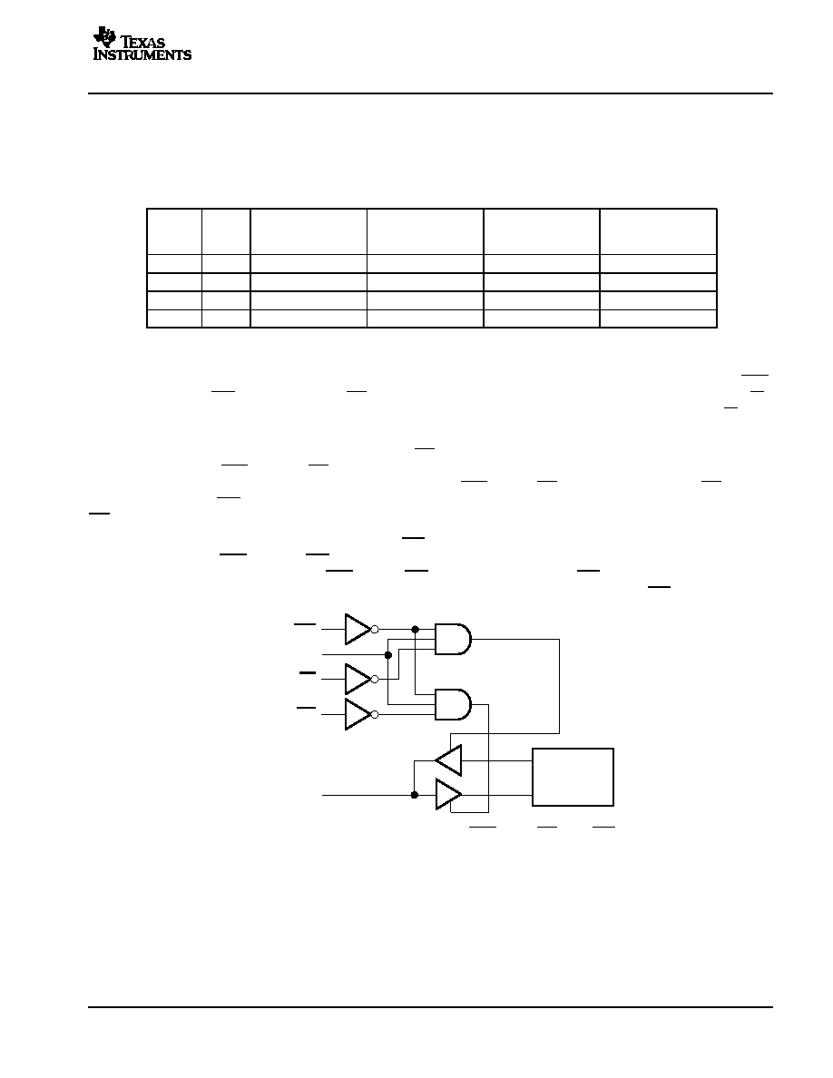
TIMING AND SIGNAL DESCRIPTION OF THE THS10064
The reading from the THS10064 and writing to the THS10064 is performed by using the chip select inputs (CS0,
CS1), the write input WR and the read input RD. The write input is configurable to a combined read/write input (R/W).
This is desired in cases where the connected processor consists of a combined read/write output signal (R/W). The
two chip select inputs can be used to interface easily to a processor.
Reading from the THS10064 takes place by an internal RDint signal, which is generated from the logical combination
of the external signals CS0, CS1 and RD (see Figure 37). This signal is then used to strobe the words out of the FIFO
and to enable the output buffers. The last external signal (either CS0, CS1 or RD) to become valid makes RDint active
while the write input (WR) is inactive. The first of those external signals going to its inactive state then deactivates
RDint again.
Writing to the THS10064 takes place by an internal WRint signal, which is generated from the logical combination
of the external signals CS0, CS1 and WR. This signal is then used to strobe the control words into the control registers
0 and 1. The last external signal (either CS0, CS1 or WR) to become valid makes WRint active while the read input
(RD) is inactive. The first of those external signals going to its inactive state then deactivates WRint again.
Read Enable
Write Enable
Control/Data
Registers
CS0
CS1
RD
WR
Data Bits
Figure 37. Logical Combination of CS0, CS1, RD, and WR
相关PDF资料 |
PDF描述 |
|---|---|
| THS10064CDAR | 4-CH 10-BIT PROPRIETARY METHOD ADC, PARALLEL ACCESS, PDSO32 |
| THS10064IDAR | 4-CH 10-BIT PROPRIETARY METHOD ADC, PARALLEL ACCESS, PDSO32 |
| THS10064IDAG4 | 4-CH 10-BIT PROPRIETARY METHOD ADC, PARALLEL ACCESS, PDSO32 |
| THS1007CDA | 4-CH 10-BIT PROPRIETARY METHOD ADC, PARALLEL ACCESS, PDSO32 |
| THS1007CDAR | 4-CH 10-BIT PROPRIETARY METHOD ADC, PARALLEL ACCESS, PDSO32 |
相关代理商/技术参数 |
参数描述 |
|---|---|
| THS10064IDAG4 | 功能描述:模数转换器 - ADC 10B 6 MSPS ADC Quad Ch. DSP/uP Interface RoHS:否 制造商:Texas Instruments 通道数量:2 结构:Sigma-Delta 转换速率:125 SPs to 8 KSPs 分辨率:24 bit 输入类型:Differential 信噪比:107 dB 接口类型:SPI 工作电源电压:1.7 V to 3.6 V, 2.7 V to 5.25 V 最大工作温度:+ 85 C 安装风格:SMD/SMT 封装 / 箱体:VQFN-32 |
| THS1007 | 制造商:TI 制造商全称:Texas Instruments 功能描述:10-BIT, 4 ANALOG INPUT, 6-MSPS, SIMULATANEOUS SAMPLING ANALOG-TO-DIGITAL CONVERTER |
| THS1007CDA | 功能描述:模数转换器 - ADC 10-Bit 6MSPS Simult Sampling Quad Ch RoHS:否 制造商:Texas Instruments 通道数量:2 结构:Sigma-Delta 转换速率:125 SPs to 8 KSPs 分辨率:24 bit 输入类型:Differential 信噪比:107 dB 接口类型:SPI 工作电源电压:1.7 V to 3.6 V, 2.7 V to 5.25 V 最大工作温度:+ 85 C 安装风格:SMD/SMT 封装 / 箱体:VQFN-32 |
| THS1007CDAG4 | 功能描述:模数转换器 - ADC 10-Bit 6MSPS Simult Sampling Quad Ch RoHS:否 制造商:Texas Instruments 通道数量:2 结构:Sigma-Delta 转换速率:125 SPs to 8 KSPs 分辨率:24 bit 输入类型:Differential 信噪比:107 dB 接口类型:SPI 工作电源电压:1.7 V to 3.6 V, 2.7 V to 5.25 V 最大工作温度:+ 85 C 安装风格:SMD/SMT 封装 / 箱体:VQFN-32 |
| THS1007CDAR | 制造商:TI 制造商全称:Texas Instruments 功能描述:10-BIT, 4 ANALOG INPUT, 6-MSPS, SIMULATANEOUS SAMPLING ANALOG-TO-DIGITAL CONVERTER |
发布紧急采购,3分钟左右您将得到回复。