- 您现在的位置:买卖IC网 > PDF目录192295 > S25FL004D0LNFI013 (SPANSION LLC) 4 Megabit CMOS 3.0 Volt Flash Memory with 50 Mhz SPI Bus Interface PDF资料下载
参数资料
| 型号: | S25FL004D0LNFI013 |
| 厂商: | SPANSION LLC |
| 元件分类: | PROM |
| 英文描述: | 4 Megabit CMOS 3.0 Volt Flash Memory with 50 Mhz SPI Bus Interface |
| 中文描述: | 4M X 1 FLASH 3V PROM, DSO8 |
| 封装: | 6 X 5 MM, LEAD FREE, MO-229, WSON-8 |
| 文件页数: | 14/36页 |
| 文件大小: | 724K |
| 代理商: | S25FL004D0LNFI013 |
第1页第2页第3页第4页第5页第6页第7页第8页第9页第10页第11页第12页第13页当前第14页第15页第16页第17页第18页第19页第20页第21页第22页第23页第24页第25页第26页第27页第28页第29页第30页第31页第32页第33页第34页第35页第36页
June 28, 2004 S25FL004D_00A0
S25FL Family (Serial Peripheral Interface) S25FL004D
21
Ad va nc e
In forma t i o n
and is 0 when it is completed. At some unspecified time before the cycle is com-
pleted, the Write Enable Latch (WEL) bit is reset.
A Sector Erase (SE) instruction applied to any memory area that is protected by
the Block Protect (BP2, BP1, BP0) bits (see Table 1) is not executed.
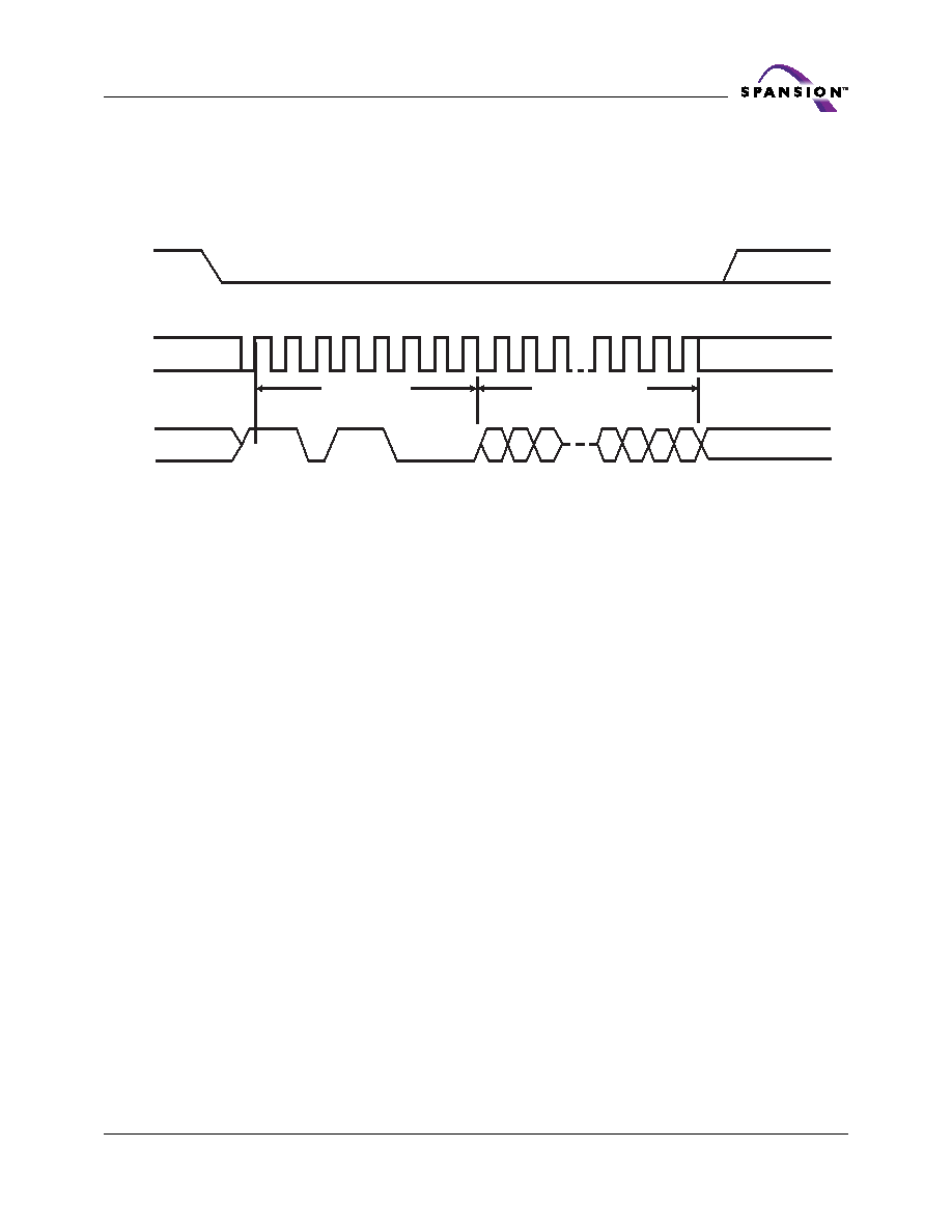
Figure 12. Sector Erase (SE) Instruction Sequence
Bulk Erase (BE)
The Bulk Erase (BE) instruction sets to 1 (FFh) all bits inside the entire memory.
Before it can be accepted, a Write Enable (WREN) instruction must previously
have been executed. After the Write Enable (WREN) instruction has been de-
coded, the device sets the Write Enable Latch (WEL).
The Bulk Erase (BE) instruction is entered by driving Chip Select (CS#) Low, fol-
lowed by the instruction code, on Serial Data Input (SI). No address is required
for the Bulk Erase (BE) instruction. Chip Select (CS#) must be driven Low for the
entire duration of the sequence.
The instruction sequence is shown in Figure 13.
Chip Select (CS#) must be driven High after the eighth bit of the last address byte
has been latched in, otherwise the Bulk Erase (BE) instruction is not executed.
As soon as Chip Select (CS#) is driven High, the self-timed Bulk Erase cycle
(whose duration is tBE) is initiated. While the Bulk Erase cycle is in progress, the
Status Register may be read to check the value of the Write In Progress (WIP)
bit. The Write In Progress (WIP) bit is 1 during the self-timed Bulk Erase cycle,
and is 0 when it is completed. At some unspecified time before the cycle is com-
pleted, the Write Enable Latch (WEL) bit is reset.
A Bulk Erase (BE) instruction is executed only if all the Block Protect (BP2, BP1,
BP0) bits (see Table 1) are set to 0. The Bulk Erase (BE) instruction is ignored if
one or more sectors are protected.
CS#
SCK
SI
Instruction
24 Bit Address
01
2
3
4
5
6
7
8
9
10
28 29 30 31
23 22 21
3
2
1
0
MSB
相关PDF资料 |
PDF描述 |
|---|---|
| S25FL004D | 4 Megabit CMOS 3.0 Volt Flash Memory with 50 Mhz SPI Bus Interface |
| S25FL004D0LNAI011 | 4 Megabit CMOS 3.0 Volt Flash Memory with 50 Mhz SPI Bus Interface |
| S25FL004D0LNAI013 | 4 Megabit CMOS 3.0 Volt Flash Memory with 50 Mhz SPI Bus Interface |
| S25FL064A0LNAI00 | 64M X 1 FLASH 3V PROM, PDSO16 |
| S2684-254 | PHOTO DIODE |
相关代理商/技术参数 |
参数描述 |
|---|---|
| S25FL004K0XMFI010 | 功能描述:闪存 4-MBIT CMOS 3V FLASH MEMORY 104MHz SPI RoHS:否 制造商:ON Semiconductor 数据总线宽度:1 bit 存储类型:Flash 存储容量:2 MB 结构:256 K x 8 定时类型: 接口类型:SPI 访问时间: 电源电压-最大:3.6 V 电源电压-最小:2.3 V 最大工作电流:15 mA 工作温度:- 40 C to + 85 C 安装风格:SMD/SMT 封装 / 箱体: 封装:Reel |
| S25FL004K0XMFI011 | 功能描述:闪存 4-MBIT CMOS 3V FLASH MEMORY 104MHz SPI RoHS:否 制造商:ON Semiconductor 数据总线宽度:1 bit 存储类型:Flash 存储容量:2 MB 结构:256 K x 8 定时类型: 接口类型:SPI 访问时间: 电源电压-最大:3.6 V 电源电压-最小:2.3 V 最大工作电流:15 mA 工作温度:- 40 C to + 85 C 安装风格:SMD/SMT 封装 / 箱体: 封装:Reel |
| S25FL004K0XMFI013 | 制造商:Spansion 功能描述:FLASH SERL-SPI 3V/3.3V 4MBIT - Bulk |
| S25FL004K0XMFI040 | 功能描述:闪存 4-MBIT CMOS 3V FLASH MEMORY 104MHz SPI RoHS:否 制造商:ON Semiconductor 数据总线宽度:1 bit 存储类型:Flash 存储容量:2 MB 结构:256 K x 8 定时类型: 接口类型:SPI 访问时间: 电源电压-最大:3.6 V 电源电压-最小:2.3 V 最大工作电流:15 mA 工作温度:- 40 C to + 85 C 安装风格:SMD/SMT 封装 / 箱体: 封装:Reel |
| S25FL004K0XMFI041 | 制造商:Spansion 功能描述:IC 4-MBIT CMOS 3.0 VOLT FLASH MEMORY 104MHZ SPI - Bulk |
发布紧急采购,3分钟左右您将得到回复。