- 您现在的位置:买卖IC网 > PDF目录18868 > MTB50P03HDLT4G (ON Semiconductor)MOSFET P-CH 30V 50A D2PAK PDF资料下载
参数资料
| 型号: | MTB50P03HDLT4G |
| 厂商: | ON Semiconductor |
| 文件页数: | 1/9页 |
| 文件大小: | 0K |
| 描述: | MOSFET P-CH 30V 50A D2PAK |
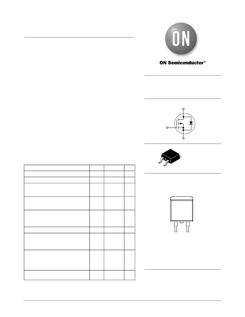
| 产品目录绘图: | MOSFET D2PAK |
| 标准包装: | 10 |
| FET 型: | MOSFET P 通道,金属氧化物 |
| FET 特点: | 逻辑电平门 |
| 漏极至源极电压(Vdss): | 30V |
| 电流 - 连续漏极(Id) @ 25° C: | 50A |
| 开态Rds(最大)@ Id, Vgs @ 25° C: | 25 毫欧 @ 25A,5V |
| Id 时的 Vgs(th)(最大): | 2V @ 250µA |
| 闸电荷(Qg) @ Vgs: | 100nC @ 5V |
| 输入电容 (Ciss) @ Vds: | 4900pF @ 25V |
| 功率 - 最大: | 2.5W |
| 安装类型: | 表面贴装 |
| 封装/外壳: | TO-263-3,D²Pak(2 引线+接片),TO-263AB |
| 供应商设备封装: | D2PAK |
| 包装: | 标准包装 |
| 产品目录页面: | 1558 (CN2011-ZH PDF) |
| 其它名称: | MTB50P03HDLT4GOSDKR |
�� �
�
�MTB50P03HDL,�
�MVB50P03HDLT4G�
�P-Channel� Power� MOSFET�
�50� A,� 30� V,� Logic� Level� D� 2� PAK�
�This� Power� MOSFET� is� designed� to� withstand� high� energy� in� the�
�avalanche� and� commutation� modes.� The� energy� efficient� design� also�
�offers� a� drain� ?� to� ?� source� diode� with� a� fast� recovery� time.� Designed� for�
�low� voltage,� high� speed� switching� applications� in� power� supplies,�
�converters� and� PWM� motor� controls,� these� devices� are� particularly�
�well� suited� for� bridge� circuits� where� diode� speed� and� commutating�
�safe� operating� areas� are� critical� and� offer� additional� safety� margin�
�against� unexpected� voltage� transients.�
�Features�
�?� Avalanche� Energy� Specified�
�?� Source� ?� to� ?� Drain� Diode� Recovery� Time� Comparable� to� a�
�Discrete� Fast� Recovery� Diode�
�?� Diode� is� Characterized� for� Use� in� Bridge� Circuits�
�?� I� DSS� and� V� DS(on)� Specified� at� Elevated� Temperature�
�?� Short� Heatsink� Tab� Manufactured� ?� Not� Sheared�
�?� Specially� Designed� Leadframe� for� Maximum� Power� Dissipation�
�?� MVB� Prefix� for� Automotive� and� Other� Applications� Requiring�
�Unique� Site� and� Control� Change� Requirements;� AEC� ?� Q101�
�http://onsemi.com�
�50� AMPERES�
�30� VOLTS�
�R� DS(on)� =� 25� m� W�
�P� ?� Channel�
�D�
�G�
�S�
�Qualified� and� PPAP� Capable�
�?� These� Devices� are� Pb� ?� Free� and� are� RoHS� Compliant�
�MAXIMUM� RATINGS� (T� C� =� 25� °� C� unless� otherwise� noted)�
�1�
�2�
�4�
�D� 2� PAK�
�CASE� 418B�
�STYLE� 2�
�Rating�
�Drain� ?� Source� Voltage�
�Drain� ?� Gate� Voltage� (R� GS� =� 1.0� M� W� )�
�Gate� ?� Source� Voltage�
�?� Continuous�
�?� Non� ?� Repetitive� (t� p� ≤� 10� ms)�
�Drain� Current� ?� Continuous�
�Drain� Current� ?� Continuous� @� 100� °� C�
�Drain� Current� ?� Single� Pulse� (t� p� ≤� 10� m� s)�
�Total� Power� Dissipation�
�Derate� above� 25� °� C�
�Total� Power� Dissipation� @� T� C� =� 25� °� C,� when�
�mounted� with� min.� recommended� pad� size�
�Operating� and� Storage� Temperature� Range�
�Single� Pulse� Drain� ?� to� ?� Source� Avalanche�
�Energy� ?� Starting� T� J� =� 25� °� C�
�(V� DD� =� 25� Vdc,� V� GS� =� 5.0� Vdc,� Peak�
�I� L� =� 50� Apk,� L� =� 1.0� mH,� R� G� =� 25� W� )�
�Thermal� Resistance�
�?� Junction� ?� to� ?� Case�
�?� Junction� ?� to� ?� Ambient�
�?� Junction� ?� to� ?� Ambient,� when� mounted� with�
�the� minimum� recommended� pad� size�
�Maximum� Lead� Temperature� for� Soldering�
�Purposes,� 1/8� ″� from� case� for� 10� seconds�
�Symbol�
�V� DSS�
�V� DGR�
�V� GS�
�V� GSM�
�I� D�
�I� D�
�I� DM�
�P� D�
�T� J� ,� T� stg�
�E� AS�
�R� q� JC�
�R� q� JA�
�R� q� JA�
�T� L�
�Value�
�30�
�30�
�±� 15�
�±� 20�
�50�
�31�
�150�
�125�
�1.0�
�2.5�
�?� 55� to� 150�
�1250�
�1.0�
�62.5�
�50�
�260�
�Unit�
�Vdc�
�Vdc�
�Vdc�
�Vpk�
�Adc�
�Apk�
�W�
�W/� °� C�
�W�
�°� C�
�mJ�
�°� C/W�
�°� C�
�3�
�MARKING� DIAGRAM�
�&� PIN� ASSIGNMENT�
�4�
�Drain�
�M� TB�
�50P03HG�
�AYWW�
�2�
�Drain�
�1� 3�
�Gate� Source�
�MTB50P03H� =� Device� Code�
�A� =� Assembly� Location�
�Y� =� Year�
�WW� =� Work� Week�
�G� =� Pb� ?� Free� Package�
�ORDERING� INFORMATION�
�Stresses� exceeding� those� listed� in� the� Maximum� Ratings� table� may� damage� the�
�device.� If� any� of� these� limits� are� exceeded,� device� functionality� should� not� be�
�assumed,� damage� may� occur� and� reliability� may� be� affected.�
�See� detailed� ordering� and� shipping� information� in� the� package�
�dimensions� section� on� page� 7� of� this� data� sheet.�
�?� Semiconductor� Components� Industries,� LLC,� 2014�
�January,� 2014� ?� Rev.� 7�
�1�
�Publication� Order� Number:�
�MTB50P03HDL/D�
�相关PDF资料 |
PDF描述 |
|---|---|
| NTB35N15T4G | MOSFET N-CH 150V 37A D2PAK |
| ASDMB-11.0592MHZ-XY-T | OSC MEMS 11.0592 MHZ SMD |
| YGM1 C517 | THERM PTC MINI-BEAD 3MM 170C |
| YQD100N1000 | THERMISTOR PTC OCP 1000 OHM 25C |
| K50-HC0CSE25.0000MR | OSCILLATOR 25.00MHZ SMD |
相关代理商/技术参数 |
参数描述 |
|---|---|
| MTB50SA | 制造商:未知厂家 制造商全称:未知厂家 功能描述:Full-Size (7.3mm or 4.7mm height) |
| MTB50SAM | 制造商:未知厂家 制造商全称:未知厂家 功能描述:Full-Size (7.3mm or 4.7mm height) |
| MTB50SAV | 制造商:未知厂家 制造商全称:未知厂家 功能描述:Full-Size (7.3mm or 4.7mm height) |
| MTB50SAVM | 制造商:未知厂家 制造商全称:未知厂家 功能描述:Full-Size (7.3mm or 4.7mm height) |
| MTB50SB | 制造商:未知厂家 制造商全称:未知厂家 功能描述:Full-Size (7.3mm or 4.7mm height) |
发布紧急采购,3分钟左右您将得到回复。