- 您现在的位置:买卖IC网 > PDF目录4040 > MPC8548ECPXAQGB (Freescale Semiconductor)MPU POWERQUICC III 783-PBGA PDF资料下载
参数资料
| 型号: | MPC8548ECPXAQGB |
| 厂商: | Freescale Semiconductor |
| 文件页数: | 35/151页 |
| 文件大小: | 0K |
| 描述: | MPU POWERQUICC III 783-PBGA |
| 产品培训模块: | MPC8548 PowerQUICC III Processors |
| 标准包装: | 1 |
| 系列: | MPC85xx |
| 处理器类型: | 32-位 MPC85xx PowerQUICC III |
| 速度: | 1.0GHz |
| 电压: | 1.1V |
| 安装类型: | 表面贴装 |
| 封装/外壳: | 783-BBGA,FCBGA |
| 供应商设备封装: | 783-FCPBGA(29x29) |
| 包装: | 托盘 |
第1页第2页第3页第4页第5页第6页第7页第8页第9页第10页第11页第12页第13页第14页第15页第16页第17页第18页第19页第20页第21页第22页第23页第24页第25页第26页第27页第28页第29页第30页第31页第32页第33页第34页当前第35页第36页第37页第38页第39页第40页第41页第42页第43页第44页第45页第46页第47页第48页第49页第50页第51页第52页第53页第54页第55页第56页第57页第58页第59页第60页第61页第62页第63页第64页第65页第66页第67页第68页第69页第70页第71页第72页第73页第74页第75页第76页第77页第78页第79页第80页第81页第82页第83页第84页第85页第86页第87页第88页第89页第90页第91页第92页第93页第94页第95页第96页第97页第98页第99页第100页第101页第102页第103页第104页第105页第106页第107页第108页第109页第110页第111页第112页第113页第114页第115页第116页第117页第118页第119页第120页第121页第122页第123页第124页第125页第126页第127页第128页第129页第130页第131页第132页第133页第134页第135页第136页第137页第138页第139页第140页第141页第142页第143页第144页第145页第146页第147页第148页第149页第150页第151页
MPC8548E PowerQUICC III Integrated Processor Hardware Specifications, Rev. 9
Freescale Semiconductor
13
Electrical Characteristics
2.1.3
Output Driver Characteristics
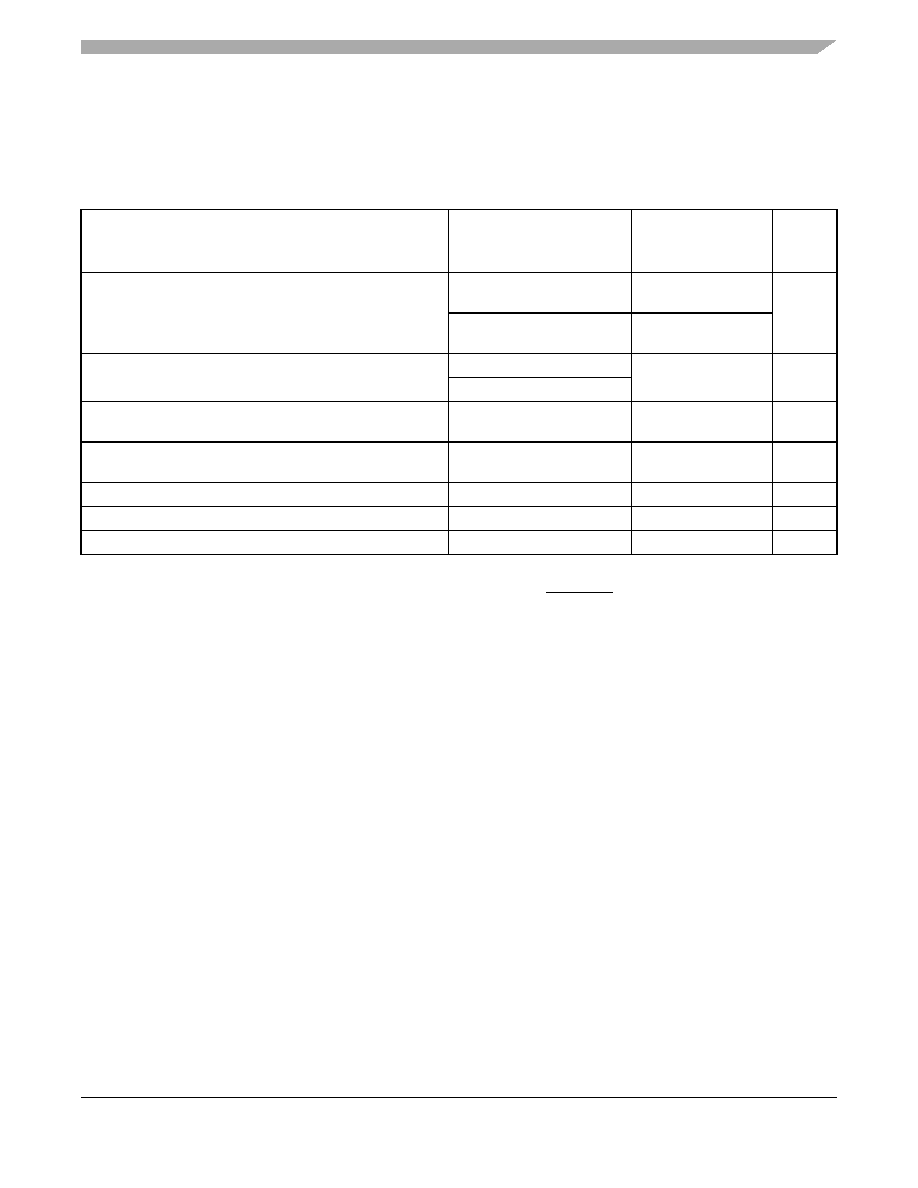
The following table provides information on the characteristics of the output driver strengths. The values
are preliminary estimates.
2.2
Power Sequencing
The device requires its power rails to be applied in a specific sequence in order to ensure proper device
operation. These requirements are as follows for power-up:
1. VDD, AVDD_n, BVDD, LVDD, OVDD, SVDD, TVDD, XVDD
2. GVDD
All supplies must be at their stable values within 50 ms.
NOTE
Items on the same line have no ordering requirement with respect to one
another. Items on separate lines must be ordered sequentially such that
voltage rails on a previous step must reach 90% of their value before the
voltage rails on the current step reach 10% of theirs.
NOTE
In order to guarantee MCKE low during power-up, the above sequencing for
GVDD is required. If there is no concern about any of the DDR signals being
in an indeterminate state during power-up, then the sequencing for GVDD is
not required.
Table 3. Output Drive Capability
Driver Type
Programmable
Output Impedance
(
)
Supply
Voltage
Notes
Local bus interface utilities signals
25
BVDD = 3.3 V
BVDD = 2.5 V
45(default)
BVDD = 3.3 V
BVDD = 2.5 V
PCI signals
25
OVDD = 3.3 V
45(default)
DDR signal
18
36 (half strength mode)
GVDD = 2.5 V
DDR2 signal
18
36 (half strength mode)
GVDD = 1.8 V
TSEC/10/100 signals
45
L/TVDD = 2.5/3.3 V
—
DUART, system control, JTAG
45
OVDD = 3.3 V
—
I2C
150
OVDD = 3.3 V
—
Notes:
1. The drive strength of the local bus interface is determined by the configuration of the appropriate bits in PORIMPSCR.
2. The drive strength of the PCI interface is determined by the setting of the PCI_GNT1 signal at reset.
3. The drive strength of the DDR interface in half-strength mode is at Tj = 105C and at GVDD (min).
相关PDF资料 |
PDF描述 |
|---|---|
| KMC8610VT1066JB | IC HOST PROCESS 1066MHZ 783-PBGA |
| FMM44DSEF-S243 | CONN EDGECARD 88POS .156 EYELET |
| MC68040FE33V | IC MICROPROCESSOR 32BIT 184-CQFP |
| IDT709089S15PF8 | IC SRAM 512KBIT 15NS 100TQFP |
| XPC8260ZUIFBC | IC MPU POWERQUICC II 480-TBGA |
相关代理商/技术参数 |
参数描述 |
|---|---|
| MPC8548ECPXAQGD | 功能描述:微处理器 - MPU PQ38 PB XT WE 1000 R3.0 RoHS:否 制造商:Atmel 处理器系列:SAMA5D31 核心:ARM Cortex A5 数据总线宽度:32 bit 最大时钟频率:536 MHz 程序存储器大小:32 KB 数据 RAM 大小:128 KB 接口类型:CAN, Ethernet, LIN, SPI,TWI, UART, USB 工作电源电压:1.8 V to 3.3 V 最大工作温度:+ 85 C 安装风格:SMD/SMT 封装 / 箱体:FBGA-324 |
| MPC8548ECPXATGB | 功能描述:微处理器 - MPU FG PQ38 8548 RoHS:否 制造商:Atmel 处理器系列:SAMA5D31 核心:ARM Cortex A5 数据总线宽度:32 bit 最大时钟频率:536 MHz 程序存储器大小:32 KB 数据 RAM 大小:128 KB 接口类型:CAN, Ethernet, LIN, SPI,TWI, UART, USB 工作电源电压:1.8 V to 3.3 V 最大工作温度:+ 85 C 安装风格:SMD/SMT 封装 / 箱体:FBGA-324 |
| MPC8548ECPXAUJB | 功能描述:微处理器 - MPU FG PQ38 8548 RoHS:否 制造商:Atmel 处理器系列:SAMA5D31 核心:ARM Cortex A5 数据总线宽度:32 bit 最大时钟频率:536 MHz 程序存储器大小:32 KB 数据 RAM 大小:128 KB 接口类型:CAN, Ethernet, LIN, SPI,TWI, UART, USB 工作电源电压:1.8 V to 3.3 V 最大工作温度:+ 85 C 安装风格:SMD/SMT 封装 / 箱体:FBGA-324 |
| MPC8548ECPXAUJC | 功能描述:微处理器 - MPU REV2.1.3 FG PART 1333 RoHS:否 制造商:Atmel 处理器系列:SAMA5D31 核心:ARM Cortex A5 数据总线宽度:32 bit 最大时钟频率:536 MHz 程序存储器大小:32 KB 数据 RAM 大小:128 KB 接口类型:CAN, Ethernet, LIN, SPI,TWI, UART, USB 工作电源电压:1.8 V to 3.3 V 最大工作温度:+ 85 C 安装风格:SMD/SMT 封装 / 箱体:FBGA-324 |
| MPC8548ECPXAUJD | 功能描述:微处理器 - MPU PQ38 PB XT WE 1333 R3.0 RoHS:否 制造商:Atmel 处理器系列:SAMA5D31 核心:ARM Cortex A5 数据总线宽度:32 bit 最大时钟频率:536 MHz 程序存储器大小:32 KB 数据 RAM 大小:128 KB 接口类型:CAN, Ethernet, LIN, SPI,TWI, UART, USB 工作电源电压:1.8 V to 3.3 V 最大工作温度:+ 85 C 安装风格:SMD/SMT 封装 / 箱体:FBGA-324 |
发布紧急采购,3分钟左右您将得到回复。