参数资料
| 型号: | LT1210CT7#PBF |
| 厂商: | Linear Technology |
| 文件页数: | 3/16页 |
| 文件大小: | 0K |
| 描述: | IC AMP C-FEEDBACK 1.1A TO-220-7 |
| 标准包装: | 50 |
| 放大器类型: | 电流反馈 |
| 电路数: | 1 |
| 转换速率: | 90 V/µs |
| -3db带宽: | 55MHz |
| 电流 - 输入偏压: | 10µA |
| 电压 - 输入偏移: | 3000µV |
| 电流 - 电源: | 35mA |
| 电流 - 输出 / 通道: | 2A |
| 电压 - 电源,单路/双路(±): | 10 V ~ 30 V,±5 V ~ 15 V |
| 工作温度: | 0°C ~ 70°C |
| 安装类型: | 通孔 |
| 封装/外壳: | TO-220-7 成形引线 |
| 供应商设备封装: | TO-220-7 |
| 包装: | 管件 |
| 产品目录页面: | 1317 (CN2011-ZH PDF) |
11
LT1210
1210fa
U
S
A
O
PPLICATI
WU
U
I FOR ATIO
Power Supplies
The LT1210 will operate from single or split supplies from
±5V (10V total) to ±15V (30V total). It is not necessary to
use equal value split supplies, however the offset voltage
and inverting input bias current will change. The offset
voltage changes about 500
V per volt of supply mis-
match. The inverting bias current can change as much as
5
A per volt of supply mismatch, though typically the
change is less than 0.5
A per volt.
Power Supply Bypassing
To obtain the maximum output and the minimum distor-
tion from the LT1210, the power supply rails should be
well bypassed. For example, with the output stage pouring
1A current peaks into the load, a 1
power supply imped-
ance will cause a droop of 1V, reducing the available
output swing by that amount. Surface mount tantalum and
ceramic capacitors make excellent low ESR bypass ele-
ments when placed close to the chip. For frequencies
above 100kHz, use 1
F and 100nF ceramic capacitors.
If significant power must be delivered below 100kHz,
capacitive reactance becomes the limiting factor. Larger
ceramic or tantalum capacitors, such as 4.7
F, are recom-
mended in place of the 1
F unit mentioned above.
Inadequate bypassing is evidenced by reduced output
swing and “distorted” clipping effects when the output is
driven to the rails. If this is observed, check the supply pins
of the device for ripple directly related to the output
waveform. Significant supply modulation indicates poor
bypassing.
Thermal Considerations
The LT1210 contains a thermal shutdown feature which
protects against excessive internal (junction) tempera-
ture. If the junction temperature of the device exceeds the
protection threshold, the device will begin cycling be-
tween normal operation and an off state. The cycling is not
harmful to the part. The thermal cycling occurs at a slow
rate, typically 10ms to several seconds, which depends on
the power dissipation and the thermal time constants of
the package and heat sinking. Raising the ambient tem-
perature until the device begins thermal shutdown gives a
good indication of how much margin there is in the
thermal design.
COPPER AREA
For surface mount devices heat sinking is accomplished
by using the heat spreading capabilities of the PC board
and its copper traces. Experiments have shown that the
heat spreading copper layer does not need to be electri-
cally connected to the tab of the device. The PCB material
can be very effective at transmitting heat between the pad
area attached to the tab of the device, and a ground or
power plane layer either inside or on the opposite side of
the board. Although the actual thermal resistance of the
PCB material is high, the length/area ratio of the thermal
resistance between the layer is small. Copper board stiff-
eners and plated through holes can also be used to spread
the heat generated by the device.
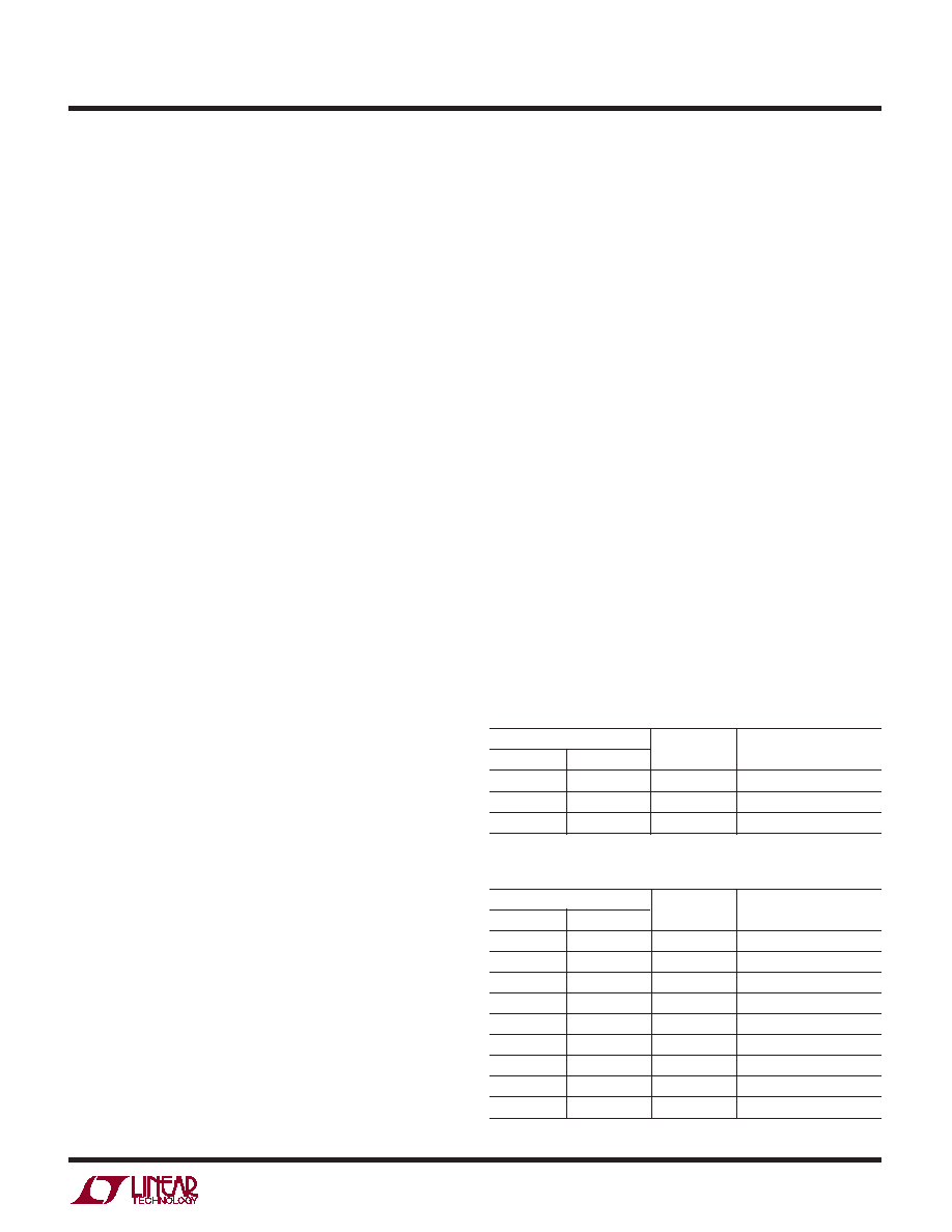
Tables 1 and 2 list thermal resistance for each package. For
the TO-220 package, thermal resistance is given for junc-
tion-to-case only since this package is usually mounted to
a heat sink. Measured values of thermal resistance for
several different board sizes and copper areas are listed for
each surface mount package. All measurements were
taken in still air on 3/32" FR-4 board with 2 oz copper. This
data can be used as a rough guideline in estimating
thermal resistance. The thermal resistance for each appli-
cation will be affected by thermal interactions with other
components as well as board size and shape.
Table 1. R Package, 7-Lead DD
THERMAL RESISTANCE
TOPSIDE*
BACKSIDE
BOARD AREA (JUNCTION-TO-AMBIENT)
2500 sq. mm
25
°C/W
1000 sq. mm
2500 sq. mm
27
°C/W
125 sq. mm
2500 sq. mm
35
°C/W
*Tab of device attached to topside copper
Table 2. Fused 16-Lead SO Package
THERMAL RESISTANCE
TOPSIDE
BACKSIDE
BOARD AREA
(JUNCTION-TO-AMBIENT)
2500 sq. mm
5000 sq. mm
40
°C/W
1000 sq. mm
2500 sq. mm
3500 sq. mm
46
°C/W
600 sq. mm
2500 sq. mm
3100 sq. mm
48
°C/W
180 sq. mm
2500 sq. mm
2680 sq. mm
49
°C/W
180 sq. mm
1000 sq. mm
1180 sq. mm
56
°C/W
180 sq. mm
600 sq. mm
780 sq. mm
58
°C/W
180 sq. mm
300 sq. mm
480 sq. mm
59
°C/W
180 sq. mm
100 sq. mm
280 sq. mm
60
°C/W
180 sq. mm
0 sq. mm
180 sq. mm
61
°C/W
COPPER AREA
相关PDF资料 |
PDF描述 |
|---|---|
| TSW-118-23-L-S | CONN HEADER 18POS .100" SGL GOLD |
| AD526JNZ | IC AMP PGA 10MA 16DIP |
| TSW-102-17-G-D | CONN HEADER 4POS .100" DUAL GOLD |
| TSW-130-07-T-S | CONN HEADER 30POS .100" SNGL TIN |
| TSW-116-07-L-S | CONN HEADER 16POS .100" SGL GOLD |
相关代理商/技术参数 |
参数描述 |
|---|---|
| LT1211 | 制造商:LINER 制造商全称:Linear Technology 功能描述:14MHz, 7V/us, Single Supply Dual and Quad Precision Op Amps |
| LT1211ACN8 | 功能描述:IC PREC OP-AMP 14MHZ DUAL 8-DIP RoHS:否 类别:集成电路 (IC) >> Linear - Amplifiers - Instrumentation 系列:- 标准包装:50 系列:- 放大器类型:J-FET 电路数:2 输出类型:- 转换速率:3.5 V/µs 增益带宽积:1MHz -3db带宽:- 电流 - 输入偏压:30pA 电压 - 输入偏移:2000µV 电流 - 电源:200µA 电流 - 输出 / 通道:- 电压 - 电源,单路/双路(±):7 V ~ 36 V,±3.5 V ~ 18 V 工作温度:0°C ~ 70°C 安装类型:通孔 封装/外壳:8-DIP(0.300",7.62mm) 供应商设备封装:8-PDIP 包装:管件 |
| LT1211ACN8#PBF | 功能描述:IC PREC OP-AMP 14MHZ DUAL 8-DIP RoHS:是 类别:集成电路 (IC) >> Linear - Amplifiers - Instrumentation 系列:- 标准包装:50 系列:- 放大器类型:J-FET 电路数:2 输出类型:- 转换速率:3.5 V/µs 增益带宽积:1MHz -3db带宽:- 电流 - 输入偏压:30pA 电压 - 输入偏移:2000µV 电流 - 电源:200µA 电流 - 输出 / 通道:- 电压 - 电源,单路/双路(±):7 V ~ 36 V,±3.5 V ~ 18 V 工作温度:0°C ~ 70°C 安装类型:通孔 封装/外壳:8-DIP(0.300",7.62mm) 供应商设备封装:8-PDIP 包装:管件 |
| LT1211AMJ8 | 制造商:Linear Technology 功能描述:OP Amp Dual GP ±18V/36V 8-Pin CDIP 制造商:Linear Technology 功能描述:OP Amp Dual GP 18V/36V 8-Pin CDIP |
| LT1211C | 制造商:LINER 制造商全称:Linear Technology 功能描述:14MHz, 7V/us, Single Supply Dual and Quad Precision Op Amps |
发布紧急采购,3分钟左右您将得到回复。