参数资料
| 型号: | LT1210CT7#PBF |
| 厂商: | Linear Technology |
| 文件页数: | 16/16页 |
| 文件大小: | 0K |
| 描述: | IC AMP C-FEEDBACK 1.1A TO-220-7 |
| 标准包装: | 50 |
| 放大器类型: | 电流反馈 |
| 电路数: | 1 |
| 转换速率: | 90 V/µs |
| -3db带宽: | 55MHz |
| 电流 - 输入偏压: | 10µA |
| 电压 - 输入偏移: | 3000µV |
| 电流 - 电源: | 35mA |
| 电流 - 输出 / 通道: | 2A |
| 电压 - 电源,单路/双路(±): | 10 V ~ 30 V,±5 V ~ 15 V |
| 工作温度: | 0°C ~ 70°C |
| 安装类型: | 通孔 |
| 封装/外壳: | TO-220-7 成形引线 |
| 供应商设备封装: | TO-220-7 |
| 包装: | 管件 |
| 产品目录页面: | 1317 (CN2011-ZH PDF) |
9
LT1210
1210fa
U
S
A
O
PPLICATI
WU
U
I FOR ATIO
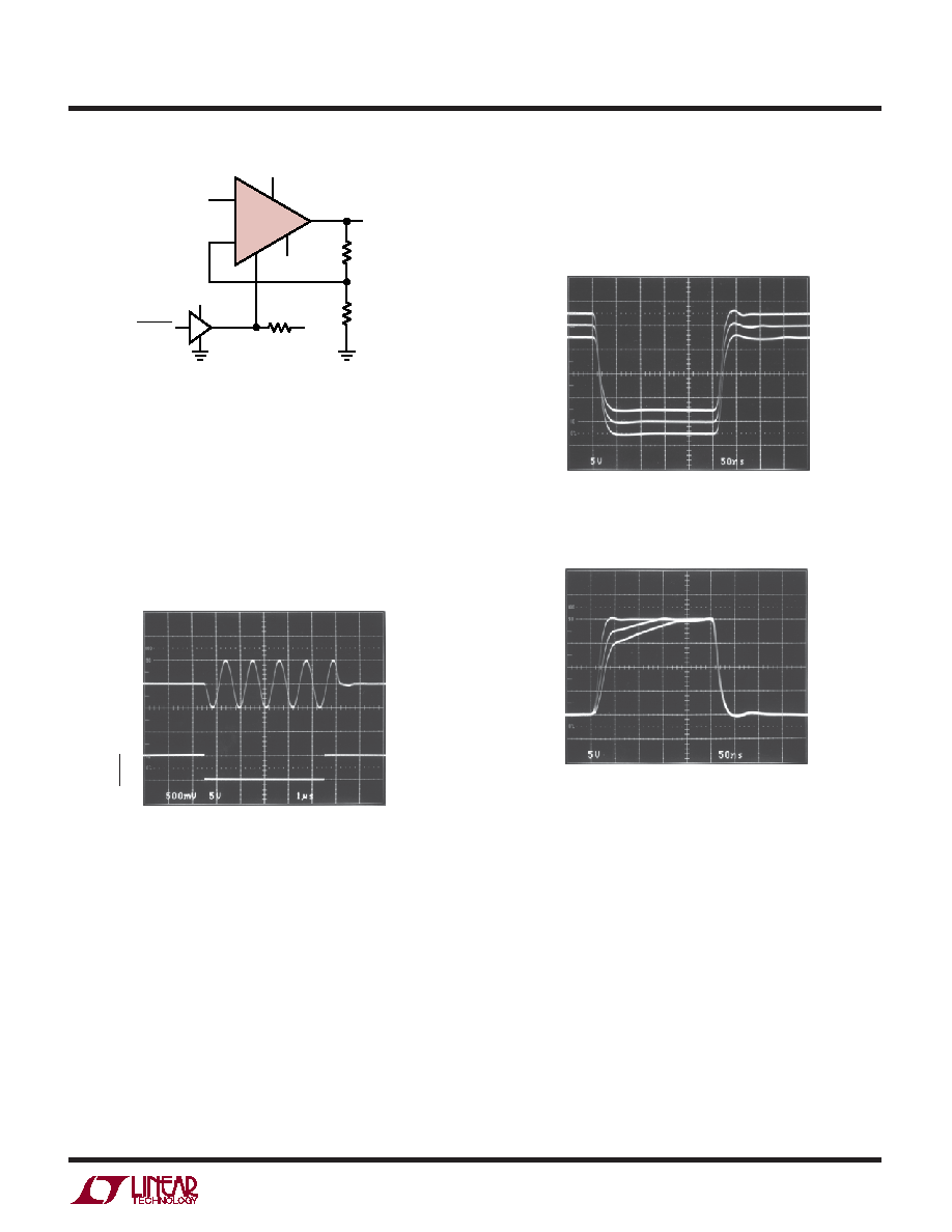
Figure 2. Shutdown Interface
–
+
LT1210
SD
15V
–15V
RF
RG
VIN
5V
24k
ENABLE
VOUT
1210 F02
15V
74C906
up the turn-off time and ensures that the LT1210 is
completely turned off. Because the pin is referenced to
the positive supply, the logic used should have a break-
down voltage of greater than the positive supply voltage.
No other circuitry is necessary as the internal circuit
limits the Shutdown pin current to about 500
A. Figure
3 shows the resulting waveforms.
Figure 3. Shutdown Operation
AV = 1
RF = 825
RL = 50
RPULL-UP = 24k
VIN = 1VP-P
VS = ±15V
V
OUT
ENABLE
1210 F03
For applications where the full bandwidth of the amplifier
is not required, the quiescent current of the device may be
reduced by connecting a resistor from the Shutdown pin
to ground. The quiescent current will be approximately 65
times the current in the Shutdown pin. The voltage across
the resistor in this condition is V+ – 3VBE. For example, a
82k resistor will set the quiescent supply current to 9mA
with VS = ±15V.
The photos in Figures 4a and 4b show the effect of
reducing the quiescent supply current on the large-signal
response. The quiescent current can be reduced to 9mA in
the inverting configuration without much change in re-
sponse. In noninverting mode, however, the slew rate is
reduced as the quiescent current is reduced.
1210 F04a
RF = 750
RL = 10
IQ = 9mA, 18mA, 36mA
VS = ±15V
Figure 4b. Large-Signal Response vs IQ, AV = 2
RF = 750
RL = 10
Figure 4a. Large-Signal Response vs IQ, AV = –1
1210 F04b
IQ = 9mA, 18mA, 36mA
VS = ±15V
Slew Rate
Unlike a traditional op amp, the slew rate of a current
feedback amplifier is not independent of the amplifier gain
configuration. There are slew rate limitations in both the
input stage and the output stage. In the inverting mode,
and for higher gains in the noninverting mode, the signal
amplitude on the input pins is small and the overall slew
rate is that of the output stage. The input stage slew rate
is related to the quiescent current and will be reduced as
the supply current is reduced. The output slew rate is set
by the value of the feedback resistors and the internal
capacitance. Larger feedback resistors will reduce the
slew rate as will lower supply voltages, similar to the way
相关PDF资料 |
PDF描述 |
|---|---|
| TSW-118-23-L-S | CONN HEADER 18POS .100" SGL GOLD |
| AD526JNZ | IC AMP PGA 10MA 16DIP |
| TSW-102-17-G-D | CONN HEADER 4POS .100" DUAL GOLD |
| TSW-130-07-T-S | CONN HEADER 30POS .100" SNGL TIN |
| TSW-116-07-L-S | CONN HEADER 16POS .100" SGL GOLD |
相关代理商/技术参数 |
参数描述 |
|---|---|
| LT1211 | 制造商:LINER 制造商全称:Linear Technology 功能描述:14MHz, 7V/us, Single Supply Dual and Quad Precision Op Amps |
| LT1211ACN8 | 功能描述:IC PREC OP-AMP 14MHZ DUAL 8-DIP RoHS:否 类别:集成电路 (IC) >> Linear - Amplifiers - Instrumentation 系列:- 标准包装:50 系列:- 放大器类型:J-FET 电路数:2 输出类型:- 转换速率:3.5 V/µs 增益带宽积:1MHz -3db带宽:- 电流 - 输入偏压:30pA 电压 - 输入偏移:2000µV 电流 - 电源:200µA 电流 - 输出 / 通道:- 电压 - 电源,单路/双路(±):7 V ~ 36 V,±3.5 V ~ 18 V 工作温度:0°C ~ 70°C 安装类型:通孔 封装/外壳:8-DIP(0.300",7.62mm) 供应商设备封装:8-PDIP 包装:管件 |
| LT1211ACN8#PBF | 功能描述:IC PREC OP-AMP 14MHZ DUAL 8-DIP RoHS:是 类别:集成电路 (IC) >> Linear - Amplifiers - Instrumentation 系列:- 标准包装:50 系列:- 放大器类型:J-FET 电路数:2 输出类型:- 转换速率:3.5 V/µs 增益带宽积:1MHz -3db带宽:- 电流 - 输入偏压:30pA 电压 - 输入偏移:2000µV 电流 - 电源:200µA 电流 - 输出 / 通道:- 电压 - 电源,单路/双路(±):7 V ~ 36 V,±3.5 V ~ 18 V 工作温度:0°C ~ 70°C 安装类型:通孔 封装/外壳:8-DIP(0.300",7.62mm) 供应商设备封装:8-PDIP 包装:管件 |
| LT1211AMJ8 | 制造商:Linear Technology 功能描述:OP Amp Dual GP ±18V/36V 8-Pin CDIP 制造商:Linear Technology 功能描述:OP Amp Dual GP 18V/36V 8-Pin CDIP |
| LT1211C | 制造商:LINER 制造商全称:Linear Technology 功能描述:14MHz, 7V/us, Single Supply Dual and Quad Precision Op Amps |
发布紧急采购,3分钟左右您将得到回复。