参数资料
| 型号: | ISL28274FAZ-T7 |
| 厂商: | Intersil |
| 文件页数: | 8/18页 |
| 文件大小: | 0K |
| 描述: | IC INSTR/OP AMP RRIO SGL 16-QSOP |
| 标准包装: | 1 |
| 放大器类型: | 仪表 |
| 电路数: | 2 |
| 输出类型: | 满摆幅 |
| 转换速率: | 0.5 V/µs |
| 增益带宽积: | 6MHz |
| 电流 - 输入偏压: | 10pA |
| 电压 - 输入偏移: | 35µV |
| 电流 - 电源: | 120µA |
| 电流 - 输出 / 通道: | 31mA |
| 电压 - 电源,单路/双路(±): | 2.4 V ~ 5 V,±1.2 V ~ 2.5 V |
| 工作温度: | -40°C ~ 125°C |
| 安装类型: | 表面贴装 |
| 封装/外壳: | 16-SSOP(0.154",3.90mm 宽) |
| 供应商设备封装: | 16-QSOP |
| 包装: | 标准包装 |
| 产品目录页面: | 1235 (CN2011-ZH PDF) |
| 其它名称: | ISL28274FAZ-T7DKR |
16
FN6345.3
May 14, 2009
Input Stage and Input Voltage Range
The input terminals (IN+ and IN-) of both amplifiers “A” and
“B” are single differential pair P-MOSFET devices aided by
an Input Range Enhancement Circuit to increase the
headroom of operation of the common-mode input voltage.
The feedback terminals (FB+ and FB-) of amplifier “A” also
have a similar topology. As a result, the input common-mode
voltage range is rail-to-rail. These amps are able to handle
input voltages that are at or slightly beyond the supply and
ground making them well suited for single 5V or 3.3V low
voltage supply systems. There is no need then to move the
common-mode input to achieve symmetrical input voltage.
Output Stage and Output Voltage Range
A pair of complementary MOSFET devices drives the output
VOUT to within a few mV of the supply rails. At a 100kΩ load,
the PMOS sources current and pulls the output up to 4mV
below the positive supply, while the NMOS sinks current and
pulls the output down to 3mV above the negative supply, or
ground in the case of a single supply operation. The current
sinking and sourcing capability of the ISL28274 are internally
limited to 31mA.
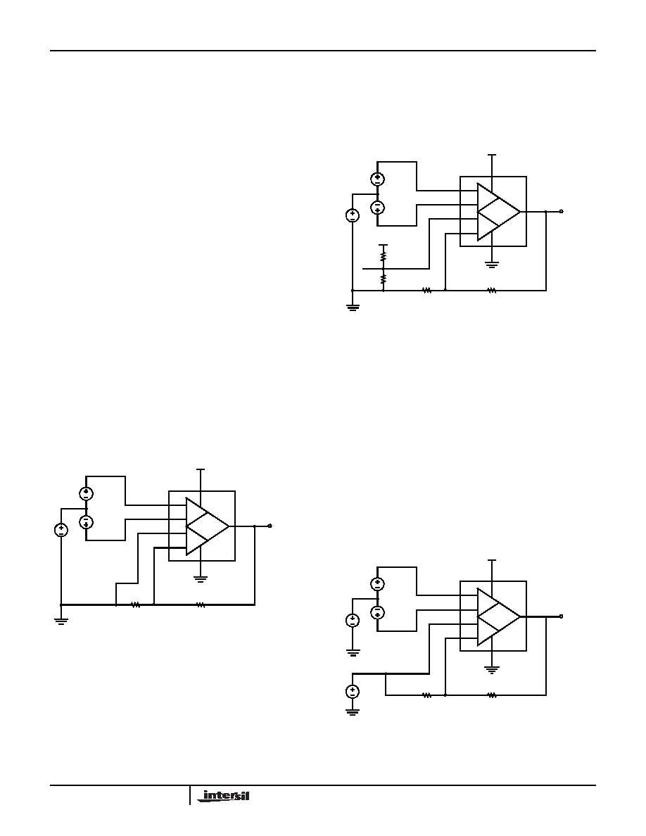
Gain Setting of Instrumentation Amp “A”
VIN, the potential difference across IN+ and IN-, is replicated
(less the input offset voltage) across FB+ and FB-. The goal
of the ISL28274 in-amp is to maintain the differential voltage
across FB+ and FB- equal to IN+ and IN-;
(FB+ - FB-) = (IN+ - IN-). Consequently, the transfer function
can be derived. The gain is set by two external resistors, the
feedback resistor RF, and the gain resistor RG.
connected to GND. With this configuration, Equation 1 is
only true for a positive swing in VIN; negative input swings
will be ignored and the output will be at ground.
Reference Connection
Unlike a three-op amp instrumentation amplifier, a finite
series resistance seen at the REF terminal does not degrade
the high CMRR performance, eliminating the need for an
additional external buffer amplifier. Figure 62 uses the FB+
pin to provide a high impedance REF terminal.
The FB+ pin is used as a REF terminal to center or to adjust
the output. Because the FB+ pin is a high impedance input,
an economical resistor divider can be used to set the voltage
at the REF terminal without degrading or affecting the CMRR
performance. Any voltage applied to the REF terminal will
shift VOUT by VREF times the closed loop gain, which is set
The FB+ pin can also be connected to the other end of resistor,
maintain constant differential voltage across the input terminals
and feedback terminals (IN+ - IN- = FB+ - FB-), the transfer
function of Figure 63 can be derived.
7
6
5
3
4
8
16
2
+
-
+
-
IN+
IN-
FB+
FB-
V+
V-
2.4V TO 5V
RF
RG
VOUT
ISL28274
VCM
VIN/2
FIGURE 61. GAIN IS BY EXTERNAL RESISTORS RF AND RG
AMP “A”
VOUT
1
R
F
R
G
--------
+
VIN
=
(EQ. 1)
FIGURE 62. GAIN SETTING AND REFERENCE CONNECTION
7
6
5
3
4
8
16
2
+
-
+
-
IN+
IN-
FB+
FB-
V+
V-
2.4V TO 5V
RF
RG
VOUT
ISL28274
VCM
VIN/2
R1
R2
REF
2.4V to 5V
AMP “A”
VOUT
1
R
F
R
G
--------
+
VIN
()
1
R
F
R
G
--------
+
VREF
()
+
=
(EQ. 2)
7
6
5
3
4
8
16
2
+
-
+
-
IN+
IN-
FB+
FB-
V+
V-
2.4V TO 5V
RF
RG
VOUT
ISL28274
VCM
VIN/2
VREF
FIGURE 63. REFERENCE CONNECTION WITH AN AVAILABLE
VREF
AMP “A”
ISL28274, ISL28474
相关PDF资料 |
PDF描述 |
|---|---|
| TA45-A341F180A4 | CIRCUIT BRKR THERMAL 18A 2POLE |
| 0459858252 | CONN HEADER 8PWR 28SGL 2.36MM |
| TA45-AHWTH140Z4-738 | CIRCUIT BRKR THERMAL 14A 2POLE |
| TA45-AHWTS070Z3 | CIRCUIT BRKR THERMAL 7A 2POLE |
| 0459841251 | CONN RCPT R/A 10PWR 28SGL 3.18MM |
相关代理商/技术参数 |
参数描述 |
|---|---|
| ISL28276 | 制造商:INTERSIL 制造商全称:Intersil Corporation 功能描述:Dual and Quad Precision Micropower Single Supply Rail-to-Rail Input and Output Precision Op Amps |
| ISL28276_07 | 制造商:INTERSIL 制造商全称:Intersil Corporation 功能描述:Dual and Quad Precision Micropower Single Supply Rail-to-Rail Input and Output Precision Op Amps |
| ISL28276EVAL1Z | 功能描述:EVALUATION BOARD FOR ISL28276 RoHS:是 类别:编程器,开发系统 >> 评估板 - 运算放大器 系列:- 产品培训模块:Lead (SnPb) Finish for COTS Obsolescence Mitigation Program 标准包装:1 系列:- |
| ISL28276FBZ | 功能描述:精密放大器 ISL28276FBZ DL 55UA RRIO PRCSN BIPOLAR RoHS:否 制造商:Maxim Integrated 每芯片的通道数量: 输入补偿电压:0.25 mV at +/- 5 V 输入电压范围(最大值): 安装风格: 封装 / 箱体:SOIC-8 Narrow 封装:Tube |
| ISL28276FBZ-T7 | 功能描述:IC OPAMP DUAL RRIO PREC 8-SOIC RoHS:是 类别:集成电路 (IC) >> Linear - Amplifiers - Instrumentation 系列:- 标准包装:500 系列:- 放大器类型:通用 电路数:4 输出类型:- 转换速率:2 V/µs 增益带宽积:5MHz -3db带宽:- 电流 - 输入偏压:100nA 电压 - 输入偏移:1500µV 电流 - 电源:1.7mA 电流 - 输出 / 通道:100mA 电压 - 电源,单路/双路(±):4 V ~ 36 V,±2 V ~ 18 V 工作温度:-40°C ~ 85°C 安装类型:通孔 封装/外壳:14-DIP(0.300",7.62mm) 供应商设备封装:14-PDIP 包装:管件 产品目录页面:1130 (CN2011-ZH PDF) 其它名称:MC33179PGOS |
发布紧急采购,3分钟左右您将得到回复。