参数资料
| 型号: | HFA1113IBZ96 |
| 厂商: | Intersil |
| 文件页数: | 13/16页 |
| 文件大小: | 0K |
| 描述: | IC BUFFER 850MHZ 8-SOIC |
| 标准包装: | 2,500 |
| 放大器类型: | 缓冲器 |
| 电路数: | 1 |
| 转换速率: | 2400 V/µs |
| -3db带宽: | 850MHz |
| 电流 - 输入偏压: | 25µA |
| 电压 - 输入偏移: | 8000µV |
| 电流 - 电源: | 21mA |
| 电流 - 输出 / 通道: | 60mA |
| 电压 - 电源,单路/双路(±): | 9 V ~ 11 V,±4.5 V ~ 5.5 V |
| 工作温度: | -40°C ~ 85°C |
| 安装类型: | 表面贴装 |
| 封装/外壳: | 8-SOIC(0.154",3.90mm 宽) |
| 供应商设备封装: | 8-SOIC |
| 包装: | 带卷 (TR) |
6
FN1342.6
July 11, 2005
.
Limiting Operation
General
The HFA1113 features user programmable output clamps to
limit output voltage excursions. Clamping action is obtained
by applying voltages to the VH and VL terminals (pins 8 and
5) of the amplifier. VH sets the upper output limit, while VL
sets the lower clamp level. If the amplifier tries to drive the
output above VH, or below VL, the clamp circuitry limits the
output voltage at VH or VL (± the clamp accuracy),
respectively. The low input bias currents of the clamp pins
allow them to be driven by simple resistive divider circuits, or
active elements such as amplifiers or DACs.
Clamp Circuitry
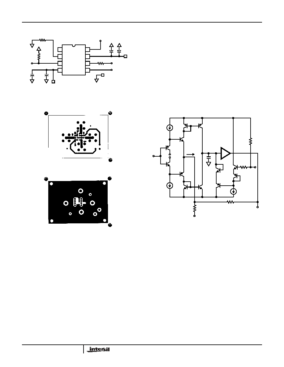
Figure 4 shows a simplified schematic of the HFA1113 input
stage, and the high clamp (VH) circuitry. As with all current
feedback amplifiers, there is a unity gain buffer (QX1 - QX2)
between the positive and negative inputs. This buffer forces
-IN to track +IN, and sets up a slewing current of:
(V-IN - VOUT)/RF + V-IN/RG
This current is mirrored onto the high impedance node (Z) by
QX3-QX4, where it is converted to a voltage and fed to the
output via another unity gain buffer. If no clamping is utilized,
the high impedance node may swing within the limits defined
by QP4 and QN4. Note that when the output reaches its
quiescent value, the current flowing through -IN is reduced to
only that small current (-IBIAS) required to keep the output at
the final voltage.
Tracing the path from VH to Z illustrates the effect of the
clamp voltage on the high impedance node. VH decreases
by 2VBE (QN6 and QP6) to set up the base voltage on QP5.
QP5 begins to conduct whenever the high impedance node
reaches a voltage equal to QP5’s base voltage + 2VBE (QP5
and QN5). Thus, QP5 clamps node Z whenever Z reaches
VH. R1 provides a pull-up network to ensure functionality
with the clamp inputs floating. A similar description applies to
the symmetrical low clamp circuitry controlled by VL.
When the output is clamped, the negative input continues to
source a slewing current (ICLAMP) in an attempt to force the
output to the quiescent voltage defined by the input. QP5
must sink this current while clamping, because the -IN
current is always mirrored onto the high impedance node.
The clamping current is calculated as:
ICLAMP = (V-IN - VOUT CLAMPED)/300 + V-IN/RG.
As an example, a unity gain circuit with VIN = 2V, and VH =1V,
would have ICLAMP = (2V - 1V)/300 +2V/∞ = 3.33mA
(RG = ∞ because -IN is floated for unity gain applications).
Note that ICC will increase by ICLAMP when the output is
clamp limited.
1
2
3
4
8
7
6
5
+5V
10
F
0.1
F
VH
50
GND
R1
-5V
0.1
F
10
F
50
IN
OUT
VL
∞ (A
V = +1)
OR 0
(AV = +2)
FIGURE 2. MODIFIED EVALUATION BOARD SCHEMATIC
VH
+IN
VL
V+
GND
1
V-
OUT
TOP LAYOUT
BOTTOM LAYOUT
FIGURE 3. EVALUATION BOARD LAYOUT
+1
+IN
V-
V+
QP1
QN1
V-
QN3
QP3
QP4
QN2
QP2
QN4
QP5
QN5
Z
V+
-IN
VOUT
ICLAMP
RF = 300
(INTERNAL)
QP6
QN6
VH
R1
50K
(30K
FOR VL)
300
RG
(INTERNAL)
V-IN
200
FIGURE 4. HFA1113 SIMPLIFIED VH CLAMP CIRCUITRY
HFA1113
相关PDF资料 |
PDF描述 |
|---|---|
| 951276-2520-AR-PR | CONN HEADER 76POS 2MM VERT SMD |
| 961244-5900-AR-PR | CONN HEADER R/A 44POS GOLD SMD |
| FTSH-117-01-F-DV-K | CONN HEADER 34POS DUAL .05" SMD |
| 155234-6203-RA | CONN HDR 2MM 34POS 10U" AU VERT |
| B1205025AEDA0GE | THERMAL PROTECTOR 50DEG C NC 6A |
相关代理商/技术参数 |
参数描述 |
|---|---|
| HFA1113IP | 制造商:Rochester Electronics LLC 功能描述:- Bulk |
| HFA1113MJ/883 | 制造商:Rochester Electronics LLC 功能描述:- Bulk |
| HFA1113ML/883 | 制造商:Intersil Corporation 功能描述:SP AMP BFFR AMP SGL 20CLCC - Rail/Tube |
| HFA1114 | 制造商:INTERSIL 制造商全称:Intersil Corporation 功能描述:850MHz Video Cable Driving Buffer |
| HFA1114EVAL | 制造商:INTERSIL 制造商全称:Intersil Corporation 功能描述:850MHz Video Cable Driving Buffer |
发布紧急采购,3分钟左右您将得到回复。