参数资料
| 型号: | AD797BRZ |
| 厂商: | Analog Devices Inc |
| 文件页数: | 7/20页 |
| 文件大小: | 0K |
| 描述: | IC OPAMP GP 110MHZ ULDIST 8SOIC |
| 标准包装: | 1 |
| 放大器类型: | 通用 |
| 电路数: | 1 |
| 转换速率: | 20 V/µs |
| 增益带宽积: | 110MHz |
| -3db带宽: | 8MHz |
| 电流 - 输入偏压: | 250nA |
| 电压 - 输入偏移: | 10µV |
| 电流 - 电源: | 8.2mA |
| 电流 - 输出 / 通道: | 50mA |
| 电压 - 电源,单路/双路(±): | ±5 V ~ 15 V |
| 工作温度: | -40°C ~ 85°C |
| 安装类型: | 表面贴装 |
| 封装/外壳: | 8-SOIC(0.154",3.90mm 宽) |
| 供应商设备封装: | 8-SO |
| 包装: | 管件 |
| 产品目录页面: | 772 (CN2011-ZH PDF) |
Data Sheet
AD797
Rev. J | Page 15 of 20
VERROR × 5
–VS
+VS
VIN
00
84
6-
0
43
TO TEKTRONIX
7A26
OSCILLOSCOPE
PREAMP INPUT
SECTION
(VIA LESS THAN 1FT
50 COAXIAL CABLE)
TEKTRONIX
CALIBRATION
FIXTURE
NOTES
USE CIRCUIT BOARD WITH GROUND PLANE.
2×
HP2835
2×
HP2835
1M
226
51pF
1k
100
250
0.47F
1F
0.1F
1F
0.1F
0.47F
4.26k
20pF
7
3
6
2
A2
AD829
A1
AD797
4
7
3
6
2
4
+
–
+
–
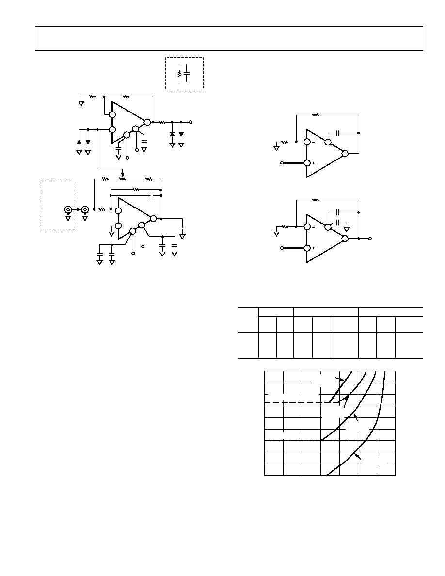
Figure 44. Settling Time Test Circuit
DISTORTION REDUCTION
The AD797 has distortion performance (THD < 120 dB,
at 20 kHz, 3 V rms, RL = 600 Ω) unequaled by most voltage
feedback amplifiers.
At higher gains and higher frequencies, THD increases due to a
reduction in loop gain. However, in contrast to most conven-
tional voltage feedback amplifiers, the AD797 provides two
effective means of reducing distortion as gain and frequency
are increased: cancellation of the distortion of the output stage
and gain bandwidth enhancement by decompensation. By
applying these techniques, gain bandwidth can be increased to
450 MHz at G = 1000, and distortion can be held to 100 dB at
20 kHz for G = 100.
The unique design of the AD797 provides cancellation of the
output stage’s distortion. To achieve this, a capacitance equal to
the effective compensation capacitance, usually 50 pF, is
connected between Pin 8 and the output (see C2 in Figure 45).
Use of this feature improves distortion performance when the
closed-loop gain is more than 10 or when frequencies of interest
are greater than 30 kHz.
Bandwidth enhancement via decompensation is achieved by
connecting a capacitor from Pin 8 to ground (see C1 in Figure 45).
Adding C1 results in subtracting from the value of the internal
compensation capacitance (50 pF), yielding a smaller effective
compensation capacitance and therefore a larger bandwidth.
The benefits of adding C1 are evident for closed-loop gains
of ≥100. A maximum value of ≈33 pF at gains of ≥1000 is
recommended. At a gain of 1000, the bandwidth is 450 kHz.
Table 8 and Figure 46 summarize the performance of the
AD797 with distortion cancellation and decompensation.
VIN
a.
b.
AD797
00
84
6-
0
44
50pF
R1
R2
C1, SEE TABLE
C2 = 50pF – C1
6
2
3
VIN
AD797
C2
C1
R1
6
2
3
8
VOUT
Figure 45. Recommended Connections for Distortion Cancellation
and Bandwidth Enhancement
Table 8. Recommended External Compensation for
Distortion Cancellation and Bandwidth Enhancement
A/B
A
B
Gain
R1
(Ω)
R2
(Ω)
C1
(pF)
C2
(pF)
3 dB
BW
C1
(pF)
C2
(pF)
3 dB
BW
10
909
100
0
50
6 MHz
0
50
6 MHz
100
1 k
10
0
50
1 MHz
15
33
1.5 MHz
1000
10 k
10
0
50
110 kHz
33
15
450 kHz
00
84
6-
0
45
–80
300k
–120
300
100
–110
–100
–90
100k
30k
10k
3k
1k
FREQUENCY (Hz)
TH
D
(
d
B
)
0.01
0.003
0.001
0.0003
0.0001
TH
D
(
%
)
NOISE LIMIT, G = +1000
NOISE LIMIT, G = +100
G = +1000
RL = 600
G = +1000
RL = 10k
G = +10
RL = 600
G = +100
RL = 600
Figure 46. Total Harmonic Distortion (THD) vs. Frequency at 3 V rms
相关PDF资料 |
PDF描述 |
|---|---|
| TMM-112-01-T-S | CONN HEADER 12POS SNGL 2MM T/H |
| TMM-111-01-T-S-SM | CONN HEADER 11POS SNGL 2MM SMD |
| TLW-110-06-T-S | CONN HEADER .100" 10POS SNGL TIN |
| TLW-110-05-T-S | CONN HEADER .100" 10POS SNGL TIN |
| TSW-112-23-T-D | CONN HEADER 24POS .100" DUAL TIN |
相关代理商/技术参数 |
参数描述 |
|---|---|
| AD797BRZ-REEL | 功能描述:IC OPAMP GP 110MHZ ULDIST 8SOIC RoHS:是 类别:集成电路 (IC) >> Linear - Amplifiers - Instrumentation 系列:- 标准包装:150 系列:- 放大器类型:音频 电路数:2 输出类型:- 转换速率:5 V/µs 增益带宽积:12MHz -3db带宽:- 电流 - 输入偏压:100nA 电压 - 输入偏移:500µV 电流 - 电源:6mA 电流 - 输出 / 通道:50mA 电压 - 电源,单路/双路(±):4 V ~ 32 V,±2 V ~ 16 V 工作温度:-40°C ~ 85°C 安装类型:表面贴装 封装/外壳:8-TSSOP(0.173",4.40mm 宽) 供应商设备封装:8-TSSOP 包装:管件 |
| AD797BRZ-REEL7 | 功能描述:IC OPAMP GP 110MHZ ULDIST 8SOIC RoHS:是 类别:集成电路 (IC) >> Linear - Amplifiers - Instrumentation 系列:- 标准包装:2,500 系列:Excalibur™ 放大器类型:J-FET 电路数:1 输出类型:- 转换速率:45 V/µs 增益带宽积:10MHz -3db带宽:- 电流 - 输入偏压:20pA 电压 - 输入偏移:490µV 电流 - 电源:1.7mA 电流 - 输出 / 通道:48mA 电压 - 电源,单路/双路(±):4.5 V ~ 38 V,±2.25 V ~ 19 V 工作温度:-40°C ~ 85°C 安装类型:表面贴装 封装/外壳:8-SOIC(0.154",3.90mm 宽) 供应商设备封装:8-SOIC 包装:带卷 (TR) |
| AD797SQ/883B | 制造商:未知厂家 制造商全称:未知厂家 功能描述:Voltage-Feedback Operational Amplifier |
| AD7980 | 制造商:AD 制造商全称:Analog Devices 功能描述:16-bit, 1 MSPS PulSAR ADC in MSOP/QFN |
| AD7980_13 | 制造商:AD 制造商全称:Analog Devices 功能描述:16-Bit, 1 MSPS PulSAR ADC in MSOP/QFN |
发布紧急采购,3分钟左右您将得到回复。