- 您现在的位置:买卖IC网 > PDF目录25515 > 951462YGLFT (INTEGRATED DEVICE TECHNOLOGY INC) PROC SPECIFIC CLOCK GENERATOR, PDSO64 PDF资料下载
参数资料
| 型号: | 951462YGLFT |
| 厂商: | INTEGRATED DEVICE TECHNOLOGY INC |
| 元件分类: | 时钟产生/分配 |
| 英文描述: | PROC SPECIFIC CLOCK GENERATOR, PDSO64 |
| 封装: | 6.10 MM, 0.50 MM PITCH, ROHS COMPLIANT, MO-153, TSSOP-64 |
| 文件页数: | 4/23页 |
| 文件大小: | 241K |
| 代理商: | 951462YGLFT |
12
Integrated
Circuit
Systems, Inc.
ICS951462
1094J—03/16/09
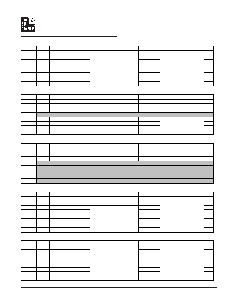
SMBus Table: Byte Count Register
Byte 8
Pin #
Name
Control Function
Type
0
1
PWD
Bit 7
-
BC7
RW
0
Bit 6
-BC6
RW
0
Bit 5
-
BC5
RW
0
Bit 4
-
BC4
RW
0
Bit 3
-
BC3
RW
1
Bit 2
-
BC2
RW
0
Bit 1
-
BC1
RW
0
Bit 0
-
BC0
RW
1
SMBus Table: REF2, 48MHz Output Strength Control and ATIG Frequency Select Register
Byte 9
Pin #
Name
Control Function
Type
0
1
PWD
Bit 7
62
REF2Str
REF2 Strength Control
RW
1X
2X
1
Bit 6
7
48MHz_1Str
48MHz_1 Strength Control
RW
1X
2X
1
Bit 5
6
48MHz_0Str
48MHz_0 Strength Control
RW
1X
2X
1
Bit 4
0
Bit 3
-
ATIG FS3
ATIG Freq Select Bit 3
RW
0
Bit 2
-
ATIG FS2
ATIG Freq Select Bit 2
RW
0
Bit 1
-
ATIG FS1
ATIG Freq Select Bit 1
RW
0
Bit 0
-
ATIG FS0
ATIG Freq Select Bit 0
RW
0
SMBus Table: PLLs M/N Programming Enable and REF1, REF0 Output Strength Control Register
Byte 10
Pin #
Name
Control Function
Type
0
1
PWD
Bit 7
-
M/N_EN
PLLs M/N Programming Enable
RW
Disable
Enable
0
Bit 6
63
REF1Str
REF1 Strength Control
RW
1X
2X
1
Bit 5
64
REF0Str
REF0 Strength Control
RW
1X
2X
1
Bit 4
0
Bit 3
0
Bit 2
0
Bit 1
0
Bit 0
0
SMBus Table: CPU PLL VCO Frequency Control Register
Byte 11
Pin #
Name
Control Function
Type
0
1
PWD
Bit 7
-
N Div8
N Divider Prog bit 8
RW
X
Bit 6
-
N Div 9
N Divider Prog bit 9
RW
X
Bit 5
-M Div5
RW
X
Bit 4
-M Div4
RW
X
Bit 3
-M Div3
RW
X
Bit 2
-M Div2
RW
X
Bit 1
-M Div1
RW
X
Bit 0
-M Div0
RW
X
SMBus Table: CPU PLL VCO Frequency Control Register
Byte 12
Pin #
Name
Control Function
Type
0
1
PWD
Bit 7
-N Div7
RW
X
Bit 6
-N Div6
RW
X
Bit 5
-N Div5
RW
X
Bit 4
-N Div4
RW
X
Bit 3
-N Div3
RW
X
Bit 2
-N Div2
RW
X
Bit 1
-N Div1
RW
X
Bit 0
-N Div0
RW
X
N Divider Programming b(7:0)
The decimal representation of
M and N Divier in Byte 11 and
12 will configure the VCO
frequency. Default at power
up = latch-in or Byte 0 Rom
table. VCO Frequency =
14.318 x [NDiv(9:0)+8] /
[MDiv(5:0)+2]
Reserved
Byte Count Programming b(7:0)
Writing to this register will
congiure how many bytes will
be read back, default is 9
bytes.
See Table 3: ATIG
Frequency Selection Table
Reserved
The decimal representation of
M and N Divier in Byte 11 and
12 will configure the VCO
frequency. Default at power
up = latch-in or Byte 0 Rom
table. VCO Frequency =
14.318 x [NDiv(9:0)+8] /
[MDiv(5:0)+2]
M Divider Programming bits
相关PDF资料 |
PDF描述 |
|---|---|
| 951464YFLFT | 240 MHz, OTHER CLOCK GENERATOR, PDSO56 |
| 951601AFLF | 66.66 MHz, PROC SPECIFIC CLOCK GENERATOR, PDSO48 |
| 951901AF | 133.34 MHz, PROC SPECIFIC CLOCK GENERATOR, PDSO48 |
| 951901AFLFT | 133.34 MHz, PROC SPECIFIC CLOCK GENERATOR, PDSO48 |
| 951 | WIRE TERMINAL |
相关代理商/技术参数 |
参数描述 |
|---|---|
| 951463AGLF | 制造商:Integrated Device Technology Inc 功能描述:951463AGLF - Rail/Tube |
| 951463BFLF | 制造商:Integrated Device Technology Inc 功能描述:PC MAIN CLOCK 制造商:Integrated Device Technology Inc 功能描述:56 SSOP (LEAD FREE) - Rail/Tube |
| 951463BFLFT | 制造商:Integrated Device Technology Inc 功能描述:PC MAIN CLOCK 制造商:Integrated Device Technology Inc 功能描述:56 SSOP (LEAD FREE) - Tape and Reel |
| 951463BGLF | 制造商:Integrated Device Technology Inc 功能描述:PC MAIN CLOCK |
| 951463BGLFT | 制造商:Integrated Device Technology Inc 功能描述:PC MAIN CLOCK |
发布紧急采购,3分钟左右您将得到回复。