- 您现在的位置:买卖IC网 > PDF目录30702 > 49LF002 (Silicon Storage Technology, Inc.) 2 Mbit / 3 Mbit / 4 Mbit / 8 Mbit Firmware Hub PDF资料下载
参数资料
| 型号: | 49LF002 |
| 厂商: | Silicon Storage Technology, Inc. |
| 英文描述: | 2 Mbit / 3 Mbit / 4 Mbit / 8 Mbit Firmware Hub |
| 中文描述: | 2兆位/ 3兆/ 4兆位/ 8兆固件集线器 |
| 文件页数: | 9/36页 |
| 文件大小: | 412K |
| 代理商: | 49LF002 |
第1页第2页第3页第4页第5页第6页第7页第8页当前第9页第10页第11页第12页第13页第14页第15页第16页第17页第18页第19页第20页第21页第22页第23页第24页第25页第26页第27页第28页第29页第30页第31页第32页第33页第34页第35页第36页
Advance Information
2 Mbit / 3 Mbit / 4 Mbit / 8 Mbit Firmware Hub
SST49LF002A / SST49LF003A / SST49LF004A / SST49LF008A
17
2001 Silicon Storage Technology, Inc.
S71161-06-000
9/01
504
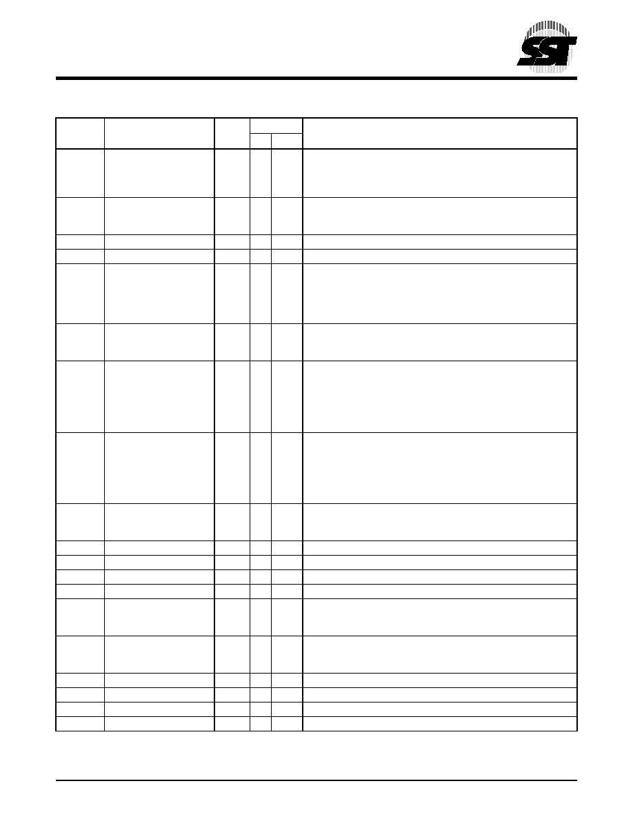
TABLE
8: PIN DESCRIPTION
Symbol
Pin Name
Type1
Interface
Functions
PP
FWH
A10-A0
Address
I
X
Inputs for low-order addresses during Read and Write operations.
Addresses are internally latched during a Write cycle. For the pro-
gramming interface, these addresses are latched by R/C# and share
the same pins as the high-order address inputs.
DQ7-DQ0
Data
I/O
X
To output data during Read cycles and receive input data during
Write cycles. Data is internally latched during a Write cycle. The out-
puts are in tri-state when OE# is high.
OE#
Output Enable
I
X
To gate the data output buffers
WE#
Write Enable
I
X
To control the Write operations
IC
Interface
Configuration Pin
I
X
This pin determines which interface is operational. When held high,
programmer mode is enabled and when held low, FWH mode is
enabled. This pin must be setup at power-up or before return from
reset and not change during device operation. This pin is internally
pulled- down with a resistor between 20-100 K
.
INIT#
Initialize
I
X
This is the second reset pin for in-system use. This pin is internally
combined with the RST# pin; If this pin or RST# pin is driven low,
identical operation is exhibited.
ID[3:0]
Identification Inputs
I
X
These four pins are part of the mechanism that allows multiple parts
to be attached to the same bus. The strapping of these pins is used
to identify the component.The boot device must have ID[3:0]=0000
and it is recommended that all subsequent devices should use
sequential up-count strapping. These pins are internally pulled-down
with a resistor between 20-100 K
.
FGPI[4:0]
General Purpose Inputs
I
X
These individual inputs can be used for additional board flexibility.
The state of these pins can be read through GPI_REG register.
These inputs should be at their desired state before the start of the
PCI clock cycle during which the read is attempted, and should
remain in place until the end of the Read cycle. Unused GPI pins
must not be floated.
TBL#
Top Block Lock
I
X
When low, prevents programming to the Boot Block sectors at top of
memory. When TBL# is high it disables hardware write protection for
the top block sectors. This pin cannot be left unconnected.
FWH[3:0]
FWH I/Os
I/O
X
I/O Communications
CLK
Clock
I
X
To provide a clock input to the control unit
FWH4
FWH Input
I
X
Input Communications
RST#
Reset
I
X
To reset the operation of the device
WP#
Write Protect
I
X
When low, prevents programming to all but the highest addressable
blocks. When WP# is high it disables hardware write protection for
these blocks. This pin cannot be left unconnected.
R/C#
Row/Column Select
I
X
Select For the Programming interface, this pin determines whether
the address pins are pointing to the row addresses, or to the column
addresses.
RES
Reserved
X
These pins must be left unconnected.
VDD
Power Supply
I
X
To provide power supply (3.0-3.6V)
VSS
Ground
I
X
Circuit ground (OV reference) Every VSS pin must be grounded.
NC
No Connection
I
X
Unconnected pins
T8.3 504
1. I = Input, O = Output
相关PDF资料 |
PDF描述 |
|---|---|
| 4A000MH5 | 2-Input NAND Gate |
| 4A002MH5 | 2-Input NOR Gate |
| 4A004MH5 | 4A004MH5 |
| 4A032MH5 | 4A032MH5 |
| 4A08P-505-500 | Surge Line Protection Module |
相关代理商/技术参数 |
参数描述 |
|---|---|
| 49LV1614-90TI | 制造商: 功能描述: 制造商:undefined 功能描述: |
| 49M-011059-FX4X10 | 制造商:Aker Technology Company Ltd 功能描述:FX4X10 Series 11.0590MHZ 30PPM 20PF SMD Crystal |
| 49M-027000-FX4X12 | 制造商:Aker Technology Company Ltd 功能描述:FX4X12 Series 27MHZ 30PPM 20PF SMD Crystal |
| 49M-10 | 制造商:Honeywell Sensing and Control 功能描述: |
| 49M1K | 功能描述:工业移动感应器和位置传感器 RESISTIVE & OPTICAL RoHS:否 制造商:Honeywell 输出类型:Analog - Current 电压额定值:12 VDC to 30 VDC 线性:+/- 0.0011 % 温度范围:- 40 C to + 85 C 总电阻: 容差: 类型:Rotary Sensor |
发布紧急采购,3分钟左右您将得到回复。