- 您现在的位置:买卖IC网 > PDF目录156551 > 37C67X (SMSC Corporation) ENHANCED SUPER I/O CONTROLLER WITH FAST IR PDF资料下载
参数资料
| 型号: | 37C67X |
| 厂商: | SMSC Corporation |
| 英文描述: | ENHANCED SUPER I/O CONTROLLER WITH FAST IR |
| 中文描述: | 增强的超级I / O控制器,快速红外线 |
| 文件页数: | 49/194页 |
| 文件大小: | 546K |
| 代理商: | 37C67X |
第1页第2页第3页第4页第5页第6页第7页第8页第9页第10页第11页第12页第13页第14页第15页第16页第17页第18页第19页第20页第21页第22页第23页第24页第25页第26页第27页第28页第29页第30页第31页第32页第33页第34页第35页第36页第37页第38页第39页第40页第41页第42页第43页第44页第45页第46页第47页第48页当前第49页第50页第51页第52页第53页第54页第55页第56页第57页第58页第59页第60页第61页第62页第63页第64页第65页第66页第67页第68页第69页第70页第71页第72页第73页第74页第75页第76页第77页第78页第79页第80页第81页第82页第83页第84页第85页第86页第87页第88页第89页第90页第91页第92页第93页第94页第95页第96页第97页第98页第99页第100页第101页第102页第103页第104页第105页第106页第107页第108页第109页第110页第111页第112页第113页第114页第115页第116页第117页第118页第119页第120页第121页第122页第123页第124页第125页第126页第127页第128页第129页第130页第131页第132页第133页第134页第135页第136页第137页第138页第139页第140页第141页第142页第143页第144页第145页第146页第147页第148页第149页第150页第151页第152页第153页第154页第155页第156页第157页第158页第159页第160页第161页第162页第163页第164页第165页第166页第167页第168页第169页第170页第171页第172页第173页第174页第175页第176页第177页第178页第179页第180页第181页第182页第183页第184页第185页第186页第187页第188页第189页第190页第191页第192页第193页第194页
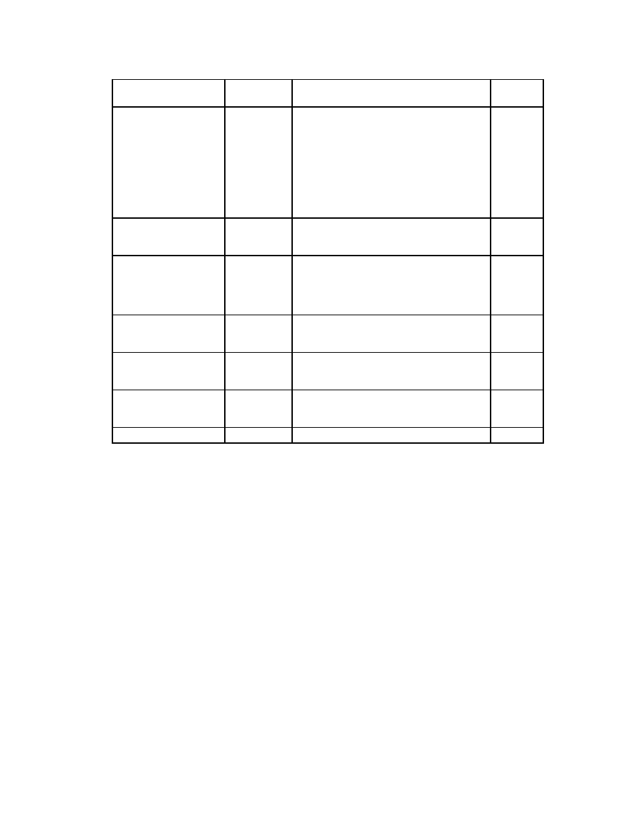
142
Table 55 - Logical Device Registers
LOGICAL DEVICE
REGISTER
ADDRESS
DESCRIPTION
STATE
Interrupt Select
Defaults :
0x70 = 0x00,
on Vcc POR or
Reset_Drv
0x72 = 0x00,
on Vcc POR or
Reset_Drv
(0x70,0x72)
0x70 is implemented for each logical device.
Refer to Interrupt Configuration Register
description.
Only the keyboard controller
uses Interrupt Select register 0x72. Unused
register (0x72) will ignore writes and return
zero when read.
Interrupts default to edge
high (ISA compatible).
C
(0x71,0x73)
Reserved - not implemented. These register
locations ignore writes and return zero when
read.
DMA Channel Select
Default = 0x04
on Vcc POR or
Reset_Drv
(0x74,0x75)
Only 0x74 is implemented for FDC, Serial
Port 2 and Parallel port.
0x75 is not
implemented and ignores writes and returns
zero when read.
Refer to DMA Channel
Configuration.
C
32-Bit Memory Space
Configuration
(0x76-0xA8)
Reserved - not implemented. These register
locations ignore writes and return zero when
read.
Logical Device
(0xA9-0xDF)
Reserved - not implemented. These register
locations ignore writes and return zero when
read.
C
Logical Device
Configuration
(0xE0-0xFE)
Reserved - Vendor Defined (see SMSC
defined
Logical
Device
Configuration
Registers).
C
Reserved
0xFF
Reserved
C
Note 1: A logical device will be active and powered up according to the following equation:
DEVICE ON (ACTIVE) = (Activate Bit SET or Pwr/Control Bit SET).
The Logical device's Activate Bit and its Pwr/Control Bit are linked such that setting
or clearing one sets or clears the other. If the I/O Base Addr of the logical device is
not within the Base I/O range as shown in the Logical Device I/O map, then read or
write is not valid and is ignored.
相关PDF资料 |
PDF描述 |
|---|---|
| 37C957FR | ULTRA I/O CONTROLLER FOR PORTABLE APPLICATIONS |
| 37FMA1-ABW31N | SPECIAL SWITCH-PIEZO SWITCH, SPST, MOMENTARY, 0.2A, 24VDC, PANEL MOUNT-THREADED |
| 37FML1-BEW31N | SPECIAL SWITCH-PIEZO SWITCH, SPST, MOMENTARY, 0.2A, 24VDC, PANEL MOUNT-THREADED |
| 37FML2-ACW21N | SPECIAL SWITCH-PIEZO SWITCH, SPST, MOMENTARY, 1A, 24VDC, PANEL MOUNT-THREADED |
| 37FMA1-AAW11N | SPECIAL SWITCH-PIEZO SWITCH, SPST, MOMENTARY, 0.2A, 24VDC, PANEL MOUNT-THREADED |
相关代理商/技术参数 |
参数描述 |
|---|---|
| 37C-6BH-5-5 | 制造商:Birtcher Products 功能描述: |
| 37C72U-185 | 制造商:White-Rodgers 功能描述: |
| 37C73U-170 | 制造商:White-Rodgers 功能描述: |
| 37C73U-171 | 制造商:White-Rodgers 功能描述: |
| 37C922BQFP | 制造商:SMSC 功能描述: |
发布紧急采购,3分钟左右您将得到回复。