参数资料
| 型号: | XCV405E-6BG560C |
| 厂商: | Xilinx Inc |
| 文件页数: | 45/118页 |
| 文件大小: | 0K |
| 描述: | IC FPGA 1.8V C-TEMP 560-MBGA |
| 产品变化通告: | FPGA Family Discontinuation 18/Apr/2011 |
| 标准包装: | 1 |
| 系列: | Virtex®-E EM |
| LAB/CLB数: | 2400 |
| 逻辑元件/单元数: | 10800 |
| RAM 位总计: | 573440 |
| 输入/输出数: | 404 |
| 门数: | 129600 |
| 电源电压: | 1.71 V ~ 1.89 V |
| 安装类型: | 表面贴装 |
| 工作温度: | 0°C ~ 85°C |
| 封装/外壳: | 560-LBGA,金属 |
| 供应商设备封装: | 560-MBGA(42.5x42.5) |
第1页第2页第3页第4页第5页第6页第7页第8页第9页第10页第11页第12页第13页第14页第15页第16页第17页第18页第19页第20页第21页第22页第23页第24页第25页第26页第27页第28页第29页第30页第31页第32页第33页第34页第35页第36页第37页第38页第39页第40页第41页第42页第43页第44页当前第45页第46页第47页第48页第49页第50页第51页第52页第53页第54页第55页第56页第57页第58页第59页第60页第61页第62页第63页第64页第65页第66页第67页第68页第69页第70页第71页第72页第73页第74页第75页第76页第77页第78页第79页第80页第81页第82页第83页第84页第85页第86页第87页第88页第89页第90页第91页第92页第93页第94页第95页第96页第97页第98页第99页第100页第101页第102页第103页第104页第105页第106页第107页第108页第109页第110页第111页第112页第113页第114页第115页第116页第117页第118页
Virtex-E 1.8 V Extended Memory Field Programmable Gate Arrays
Module 2 of 4
DS025-2 (v3.0) March 21, 2014
28
R
— OBSOLETE — OBSOLETE — OBSOLETE — OBSOLETE —
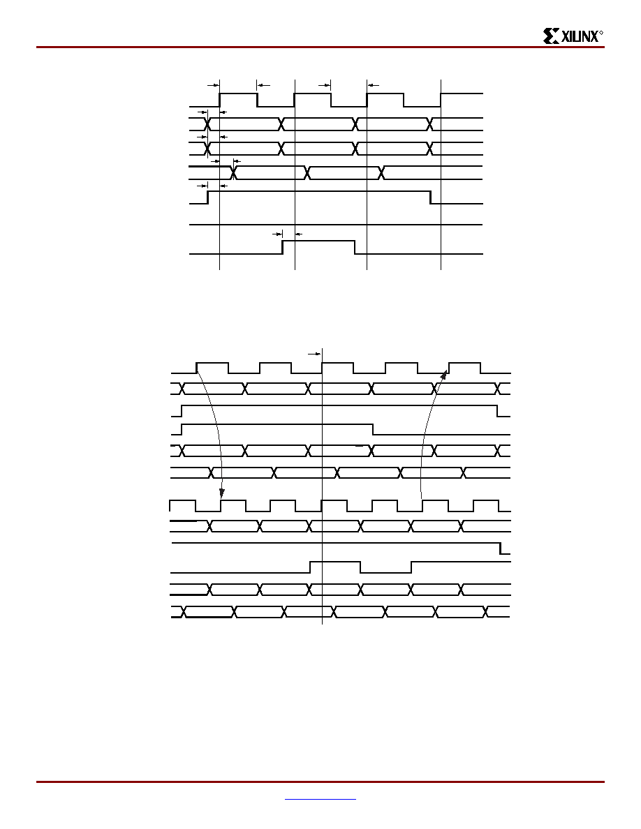
At the third rising edge of CLKA, the TBCCS parameter is
violated with two writes to memory location 0x0F. The DOA
and DOB busses reflect the contents of the DIA and DIB
busses, but the stored value at 0x0F is invalid.
At the fourth rising edge of CLKA, a read operation is per-
formed at memory location 0x0F and invalid data is present
on the DOA bus. Port B also executes a read operation to
memory location 0x0F and also reads invalid data.
At the fifth rising edge of CLKA a read operation is per-
formed that does not violate the TBCCS parameter to the
previous write of 0x7E by Port B. THe DOA bus reflects the
recently written value by Port B.
Figure 33: Timing Diagram for Single Port Block SelectRAM+ Memory
ds022_0343_121399
CLK
TBPWH
TBACK
ADDR
00
DDDD
MEM (00)
CCCC
MEM (7E)
0F
CCCC
7E
8F
BBBB
2222
DIN
DOUT
EN
RST
WE
DISABLED
READ
WRITE
READ
DISABLED
TBDCK
TBECK
TBWCK
TBCKO
TBPWL
Figure 34: Timing Diagram for a True Dual-port Read/Write Block SelectRAM+ Memory
ds022_035_121399
CLK_A
PORT
A
PORT
B
ADDR_A
00
7E
0F
00
7E
1A
0F
7E
AAAA
9999
AAAA
0000
1111
2222
AAAA
9999
AAAA
UNKNOWN
EN_A
WE_A
DI_A
DO_A
1111
2222
FFFF
BBBB
1111
AAAA
MEM (00)
9999
2222
FFFF
BBBB
UNKNOWN
CLK_B
ADDR_B
EN_B
WE_B
DI_B
DO_B
TBCCS
VIOLATION
TBCCS
相关PDF资料 |
PDF描述 |
|---|---|
| HMC43DRAS | CONN EDGECARD 86POS R/A .100 SLD |
| AMM36DSEN | CONN EDGECARD 72POS .156 EYELET |
| AMM36DSEH | CONN EDGECARD 72POS .156 EYELET |
| AMM36DRTN | CONN EDGECARD 72POS DIP .156 SLD |
| AMM36DRTH | CONN EDGECARD 72POS DIP .156 SLD |
相关代理商/技术参数 |
参数描述 |
|---|---|
| XCV405E-6BG560I | 功能描述:IC FPGA 1.8V 560-MBGA RoHS:否 类别:集成电路 (IC) >> 嵌入式 - FPGA(现场可编程门阵列) 系列:Virtex®-E EM 产品变化通告:Step Intro and Pkg Change 11/March/2008 标准包装:1 系列:Virtex®-5 SXT LAB/CLB数:4080 逻辑元件/单元数:52224 RAM 位总计:4866048 输入/输出数:480 门数:- 电源电压:0.95 V ~ 1.05 V 安装类型:表面贴装 工作温度:-40°C ~ 100°C 封装/外壳:1136-BBGA,FCBGA 供应商设备封装:1136-FCBGA 配用:568-5088-ND - BOARD DEMO DAC1408D750122-1796-ND - EVALUATION PLATFORM VIRTEX-5 |
| XCV405E-6BG676C | 制造商:XILINX 制造商全称:XILINX 功能描述:Virtex-E 1.8 V Extended Memory Field Programmable Gate Arrays |
| XCV405E-6BG676I | 制造商:XILINX 制造商全称:XILINX 功能描述:Virtex-E 1.8 V Extended Memory Field Programmable Gate Arrays |
| XCV405E-6BG900C | 制造商:XILINX 制造商全称:XILINX 功能描述:Virtex-E 1.8 V Extended Memory Field Programmable Gate Arrays |
| XCV405E-6BG900I | 制造商:XILINX 制造商全称:XILINX 功能描述:Virtex-E 1.8 V Extended Memory Field Programmable Gate Arrays |
发布紧急采购,3分钟左右您将得到回复。