- 您现在的位置:买卖IC网 > PDF目录10775 > X79000V20IT1 (Intersil)IC DAC NV SELECT OUT/MEM 20TSSOP PDF资料下载
参数资料
| 型号: | X79000V20IT1 |
| 厂商: | Intersil |
| 文件页数: | 13/18页 |
| 文件大小: | 0K |
| 描述: | IC DAC NV SELECT OUT/MEM 20TSSOP |
| 标准包装: | 2,500 |
| 设置时间: | 6µs |
| 位数: | 12 |
| 数据接口: | 串行 |
| 转换器数目: | 1 |
| 电压电源: | 单电源 |
| 工作温度: | -40°C ~ 85°C |
| 安装类型: | 表面贴装 |
| 封装/外壳: | 20-TSSOP(0.173",4.40mm 宽) |
| 供应商设备封装: | 20-TSSOP |
| 包装: | 带卷 (TR) |
| 输出数目和类型: | 1 电压,单极 |
| 采样率(每秒): | 417k |
4
FN8147.0
March 17, 2005
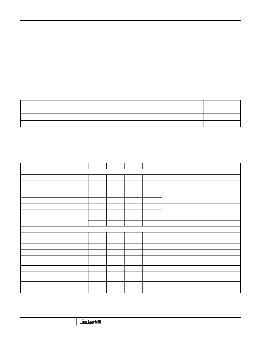
ABSOLUTE MAXIMUM RATINGS
All voltages are referred to Vss
Temperature under bias ........................ -40°C to 85°C
Storage temperature ......................... -65°C to +150°C
Voltage on every pin except Vcc ............. -0.5V to +7V
Voltage on Vcc Pin .....................................-0.5V to 6V
D.C. Output Current at pins SO and RDY............ 5 mA
D.C. Output Current at pins VL, VH,
VFB, Vout and Vref ............................. -0.50 to 1 mA
VBUF output short circuit duration............. 10 seconds
Lead temperature (soldering, 10 seconds) ........ 300°C
COMMENT
Stresses above those listed under “Absolute Maximum
Ratings” may cause permanent damage to the device.
This is a stress rating only; functional operation of the
device (at these or an other conditions above those
listed in the operational sections of this specification) is
not implied. Exposure to absolute maximum rating
conditions for extended periods may affect device
reliability.
RECOMMENDED OPERATING CONDITIONS
ELECTRICAL CHARACTERISTICS
(Unless otherwise specified, all typical values are for 25°C ambient temperature and 5V at pin Vcc. Maximum and minimum
specifications are over the recommended operating conditions. All voltages are referred to the voltage at pin Vss. All bits in
control registers are “0”. SPI interface in “standby” (see notes 1 and 2 on page 6). Output pins unloaded. Input pins floating.
DAC input is 000hex.)
Parameter
Min.
Max.
Units
Temperature
-40
+85
°C
Voltage on Vcc Pin
4.5
5.5
V
Voltage on any other Pin
-0.3
Vcc +0.3
V
Parameter
Min
Typ
Max
Units
Notes
Buffered DAC and Reference
Resolution
12
bit
INL
±10
LSB
(1)(2)(3) VL = 0.151V, VH = 3.025V
DNL
-0.5
0.5
LSB
Total Offset Error
12
mV
(1)(2)(4) VL = 0.151V, VH = 3.025V
Total Fullscale Error
22
mV
Total Offset Error Drift
50
ppm/°C
(1)(2)(4) VL = 0.151V, VH = 3.025V
Total Fullscale Error Drift
50
ppm/°C
Settling time to 1 LSB
2
10
s
Step size
≤ 100mV (2)(5)
6
30
s
Step size up to full scale (2)(5)
Buffer Only
Output Buffer Offset
-6
6
mV
150mV < Vout < VCC - 150mV
Output Buffer Offset Drift
-20
20
V/°C
(5)
DC PSRR
-1.5
+1.5
mV/V
(5)
Vbuf output slew rate
0.2
V/s
Output Buffer 3dB Bandwidth
300
1000
kHz
150mV < (V(VFB) =
V(Vbuf)) < VCC – 150mV (5)
Digital feed through
10
nVsec
(6)
Output load regulation
-1
1
mV/mA
140mV
≤ V(Vbuf) ≤ V
CC-140mV
I(Vbuf) = ±1mA
Short circuit current @ Vbuf
50
mA
V(Vbuf) = VCC or 0V
Capacitive Loading Stability
100
pF
Rload
≥ 2k (5)
X79000, X79001, X79002
相关PDF资料 |
PDF描述 |
|---|---|
| VE-J6B-MW-F1 | CONVERTER MOD DC/DC 95V 100W |
| B37931K9223K060 | CAP CER 0.022UF 16V 10% X7R 0603 |
| X79000V20I | IC DAC NV SELECT OUT/MEM 20TSSOP |
| VE-J63-MW-F3 | CONVERTER MOD DC/DC 24V 100W |
| ISL5961/2IA | IC DAC 14BIT 210MSPS 28-TSSOP |
相关代理商/技术参数 |
参数描述 |
|---|---|
| X79001 | 制造商:INTERSIL 制造商全称:Intersil Corporation 功能描述:NV DAC with Selectable Output Range and Memory |
| X79001V20I | 功能描述:IC DAC NV SELECT OUT/MEM 20TSSOP RoHS:否 类别:集成电路 (IC) >> 数据采集 - 数模转换器 系列:- 标准包装:2,400 系列:- 设置时间:- 位数:18 数据接口:串行 转换器数目:3 电压电源:模拟和数字 功率耗散(最大):- 工作温度:-40°C ~ 85°C 安装类型:表面贴装 封装/外壳:36-TFBGA 供应商设备封装:36-TFBGA 包装:带卷 (TR) 输出数目和类型:* 采样率(每秒):* |
| X79001V20IT1 | 功能描述:IC DAC NV SELECT OUT/MEM 20TSSOP RoHS:否 类别:集成电路 (IC) >> 数据采集 - 数模转换器 系列:- 标准包装:2,400 系列:- 设置时间:- 位数:18 数据接口:串行 转换器数目:3 电压电源:模拟和数字 功率耗散(最大):- 工作温度:-40°C ~ 85°C 安装类型:表面贴装 封装/外壳:36-TFBGA 供应商设备封装:36-TFBGA 包装:带卷 (TR) 输出数目和类型:* 采样率(每秒):* |
| X79002 | 制造商:INTERSIL 制造商全称:Intersil Corporation 功能描述:NV DAC with Selectable Output Range and Memory |
| X79002V20I | 功能描述:IC DAC NV SELECT OUT/MEM 20TSSOP RoHS:否 类别:集成电路 (IC) >> 数据采集 - 数模转换器 系列:- 标准包装:2,400 系列:- 设置时间:- 位数:18 数据接口:串行 转换器数目:3 电压电源:模拟和数字 功率耗散(最大):- 工作温度:-40°C ~ 85°C 安装类型:表面贴装 封装/外壳:36-TFBGA 供应商设备封装:36-TFBGA 包装:带卷 (TR) 输出数目和类型:* 采样率(每秒):* |
发布紧急采购,3分钟左右您将得到回复。