- 您现在的位置:买卖IC网 > PDF目录18734 > UPC8172TB-A (CEL)IC FREQ UP-CNVRTR 6-SMINI PDF资料下载
参数资料
| 型号: | UPC8172TB-A |
| 厂商: | CEL |
| 文件页数: | 2/11页 |
| 文件大小: | 0K |
| 描述: | IC FREQ UP-CNVRTR 6-SMINI |
| 产品目录绘图: | NE69, UP Series |
| 标准包装: | 1 |
| 系列: | UPC8172TB |
| RF 型: | 手机,DCS,PCS,W-CDMA,WLAN |
| 频率: | 50MHz ~ 400MHz |
| 混频器数目: | 1 |
| 增益: | 9.5dB |
| 噪音数据: | 9.5dB |
| 次要属性: | 升频器 |
| 电流 - 电源: | 13mA |
| 电源电压: | 2.7 V ~ 3.3 V |
| 包装: | 散装 |
| 封装/外壳: | 6-TSSOP,SC-88,SOT-363 |
| 供应商设备封装: | 6-SuperMiniMold |
| 产品目录页面: | 577 (CN2011-ZH PDF) |
�� �
�
�UPC8172TB�
�ABSOLUTE� MAXIMUM� RATINGS� 1�
�(T� A� =� +25°C� unless� otherwise� specified)�
�SYMBOLS� PARAMETERS� UNITS�
�V� CC� Supply� Voltage� V�
�RATINGS�
�3.6�
�RECOMMENDED�
�OPERATING� CONDITIONS�
�SYMBOLS� PARAMETERS� UNITS� MIN�
�V� CC� Supply� Voltage� 1� V� 2.7�
�TYP� MAX�
�3.0� 3.3�
�V� PS�
�PS� Pin� Input� Voltage�
�V�
�3.6�
�T� A�
�Operating�
�P� D�
�Power� Dissipation� 2�
�mW�
�270�
�Ambient� Temperature�
�?� C�
�-40�
�+25�
�+85�
�T� A�
�Operating� Ambient�
�°C�
�-40� to� +85�
�P� LOin�
�Local� Input� Level� 2�
�dBm�
�-10�
�-5�
�0�
�Temperature�
�f� RFout�
�RF� Output� Frequency� 3�
�GHz�
�0.8�
�–�
�2.5�
�T� STG�
�Storage� Temperature�
�°C�
�-55� to� +150�
�f� IFin�
�IF� Input� Frequency�
�MHz�
�50�
�–�
�400�
�P� IN�
�Input� Power�
�dBm�
�+10�
�Note:�
�Notes:�
�1.� Operation� in� excess� of� any� one� of� these� conditions� may� result� in�
�permanent� damage.�
�1.� Same� voltage� applied� to� pins� 5� and� 6.�
�2.� Z� S� =� 50� ?� (without� matching).�
�3.� With� external� matching� circuit.�
�2.� Mounted� on� a� double-sided� copper� clad� 50x50x1.6� mm� epoxy�
�glass� PWB,� T� A� =� +85°C.�
�SERIES� PRODUCTS� 1� (T� A� =� +25°C,� V� CC� =� V� RFout� =� 3.0� V,� Z� S� =� Z� L� =� 50� ?� )�
�Part� Number�
�I� CC�
�f� RFout�
�CG� (dB�
�OIP� 3� (dBm)�
�(mA)�
�(GHz)�
�@RF� 0.9� GHz� 2�
�@RF� 1.9� GHz�
�@RF� 2.4� GHz�
�@RF� 0.9� GHz� 2�
�@RF� 1.9� GHz�
�@RF� 2.4� GHz�
�UPC8172TB�
�UPC8106TB�
�UPC8109TB�
�UPC8163TB�
�9�
�9�
�5�
�16.5�
�0.8� to� 2.5�
�0.4� to� 2.0�
�0.4� to� 2.0�
�0.8� to� 2.0�
�9.5�
�9�
�6�
�9�
�8.5�
�7�
�4�
�5.5�
�8.0�
�–�
�–�
�–�
�+7.5�
�+5.5�
�+1.5�
�+9.5�
�+6.0�
�-1.0�
�+2.0�
�+6.0�
�+4.0�
�–�
�–�
�–�
�Notes:�
�1.� Typical� performance.�
�2.� f� RFout� =� 0.83� GHz� @� UPC8163TB�
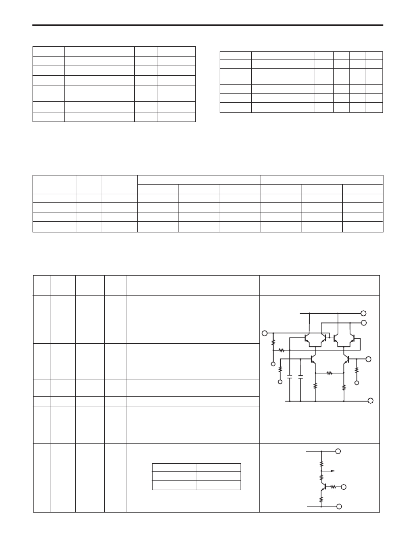
�PIN� FUNCTIONS� (Voltage� is� measured� at� V� CC� =� V� PS� =� V� RFOUT� =� 3.0� V)�
�Pin�
�No.�
�Pin�
�Name�
�Applied�
�Voltage�
�Pin�
�Voltage�
�Function� and� Explanation�
�Equivalent� Circuit�
�(V)�
�(V)�
�1�
�IFinput�
�—�
�1.4�
�This� pin� is� the� IF� input� pin� to� the� double� balanced�
�mixer� (DBM).� The� input� is� designed� as� a� high�
�impedance.� The� circuit� helps� suppress� spurious�
�signals.� Also� this� symmetrical� circuit� can� keep�
�specified� performance� insensitive� to� process-�
�condition� distribution.� For� that� reason,� a� double�
�balanced� mixer� is� adopted.�
�3�
�5�
�6�
�2�
�GND�
�GND�
�—�
�GND� pin.� Ground� pattern� on� the� board� should� be�
�formed� as� wide� as� possible.� Track� length� should�
�be� kept� as� short� as� possible� to� minimize� ground�
�inductance.�
�1�
�3�
�LOinput�
�–�
�2.3�
�Local� input� pin.� Recommendable� input� level� is� -10�
�to� 0� dBm.�
�5�
�V� CC�
�2.7� to� 3.3�
�—�
�Supply� voltage� pin.�
�2�
�6�
�RFoutput� Same� bias�
�as� V� CC�
�through�
�external�
�inductor�
�—�
�This� pin� is� the� RF� output� from� the� double�
�balanced� mixer.� This� pin� is� designed� as� an� open�
�collector.� Due� to� the� high� impedance� output,� this�
�pin� should� be� externally� equipped� with� an� LC�
�matching� circuit� to� the� next� stage.�
�4�
�PS�
�V� CC� /GND�
�Power� save� control� pin.� Bias� controls� operate� as�
�follows:�
�V� CC�
�5�
�Pin� Bias�
�V� CC�
�Control�
�Operation�
�GND�
�Power� Save�
�GND�
�2�
�4�
�相关PDF资料 |
PDF描述 |
|---|---|
| MAX19995ETX+ | IC DOWNCONVERTER 2CH 36TQFN |
| DP1283C868 | MODULE DROP IN FOR XE1283 868MHZ |
| MAX2681EUT+T | IC SIGE DOWNCONV MIXER SOT23-6 |
| DP1283C433 | MODULE DROP IN FOR XE1283 433MHZ |
| CSX750FCC18.432M-UT | OSCILLATOR 18.4320 MHZ SMD |
相关代理商/技术参数 |
参数描述 |
|---|---|
| UPC8172TB-E3 | 功能描述:上下转换器 2.5GHZ FREQ UP CONV RoHS:否 制造商:Texas Instruments 产品:Down Converters 射频:52 MHz to 78 MHz 中频:300 MHz LO频率: 功率增益: P1dB: 工作电源电压:1.8 V, 3.3 V 工作电源电流:120 mA 最大功率耗散:1 W 最大工作温度:+ 85 C 安装风格:SMD/SMT 封装 / 箱体:PQFP-128 |
| UPC8172TB-E3-A | 功能描述:上下转换器 2.5GHz Freq Upconvrt RoHS:否 制造商:Texas Instruments 产品:Down Converters 射频:52 MHz to 78 MHz 中频:300 MHz LO频率: 功率增益: P1dB: 工作电源电压:1.8 V, 3.3 V 工作电源电流:120 mA 最大功率耗散:1 W 最大工作温度:+ 85 C 安装风格:SMD/SMT 封装 / 箱体:PQFP-128 |
| UPC8172TB-EV09 | 功能描述:射频开发工具 For UPC8172TB 900MHz RoHS:否 制造商:Taiyo Yuden 产品:Wireless Modules 类型:Wireless Audio 工具用于评估:WYSAAVDX7 频率: 工作电源电压:3.4 V to 5.5 V |
| UPC8172TB-EV19 | 功能描述:射频开发工具 For UPC8172TB 1.9GHz RoHS:否 制造商:Taiyo Yuden 产品:Wireless Modules 类型:Wireless Audio 工具用于评估:WYSAAVDX7 频率: 工作电源电压:3.4 V to 5.5 V |
| UPC8172TB-EV24 | 功能描述:射频开发工具 For UPC8172TB 2.4GHz RoHS:否 制造商:Taiyo Yuden 产品:Wireless Modules 类型:Wireless Audio 工具用于评估:WYSAAVDX7 频率: 工作电源电压:3.4 V to 5.5 V |
发布紧急采购,3分钟左右您将得到回复。