- 您现在的位置:买卖IC网 > PDF目录98219 > THS1209CDAG4 (TEXAS INSTRUMENTS INC) 2-CH 12-BIT PROPRIETARY METHOD ADC, PARALLEL ACCESS, PDSO32 PDF资料下载
参数资料
| 型号: | THS1209CDAG4 |
| 厂商: | TEXAS INSTRUMENTS INC |
| 元件分类: | ADC |
| 英文描述: | 2-CH 12-BIT PROPRIETARY METHOD ADC, PARALLEL ACCESS, PDSO32 |
| 封装: | GREEN, PLASTIC, TSSOP-32 |
| 文件页数: | 6/33页 |
| 文件大小: | 312K |
| 代理商: | THS1209CDAG4 |
第1页第2页第3页第4页第5页当前第6页第7页第8页第9页第10页第11页第12页第13页第14页第15页第16页第17页第18页第19页第20页第21页第22页第23页第24页第25页第26页第27页第28页第29页第30页第31页第32页第33页
THS1209
SLAS288B – JULY 2000 – REVISED DECEMBER 2002
www.ti.com
14
DETAILED DESCRIPTION
Reference Voltage
The THS1209 has a built-in reference, which provides the reference voltages for the ADC. VREFP is set to 3.5 V
and VREFM is set to 1.5 V. An external reference can also be used through two reference input pins, REFP and
REFM, if the reference source is programmed as external. The voltage levels applied to these pins establish the
upper and lower limits of the analog inputs to produce a full-scale and zero-scale reading respectively.
Analog Inputs
The THS1209 consists of two analog inputs, which are sampled simultaneously. These inputs can be selected
individually and configured as single-ended or differential inputs. The desired analog input channel can be
programmed.
Converter
The THS1209 uses a 12-bit pipelined multistaged architecture which achieves a high sample rate with low power
consumption. The THS1209 distributes the conversion over several smaller ADC sub-blocks, refining the conversion
with progressively higher accuracy as the device passes the results from stage to stage. This distributed conversion
requires a small fraction of the number of comparators used in a traditional flash ADC. A sample-and-hold amplifier
(SHA) within each of the stages permits the first stage to operate on a new input sample while the second through
the eighth stages operate on the seven preceding samples.
Conversion
An external clock signal with a duty cycle of 50% has to be applied to the clock input (CONV_CLK). A new conversion
is started with every falling edge of the applied clock signal. The conversion values are available at the output with
a latency of 5 clock cycles.
SYNC
In multichannel mode, the first SYNC signal is delayed by [7+ (# Channels Sampled)] cycles of the CONV_CLK after
a SYNC reset. This is due to the latency of the pipeline architecture of the THS1209.
Sampling Rate
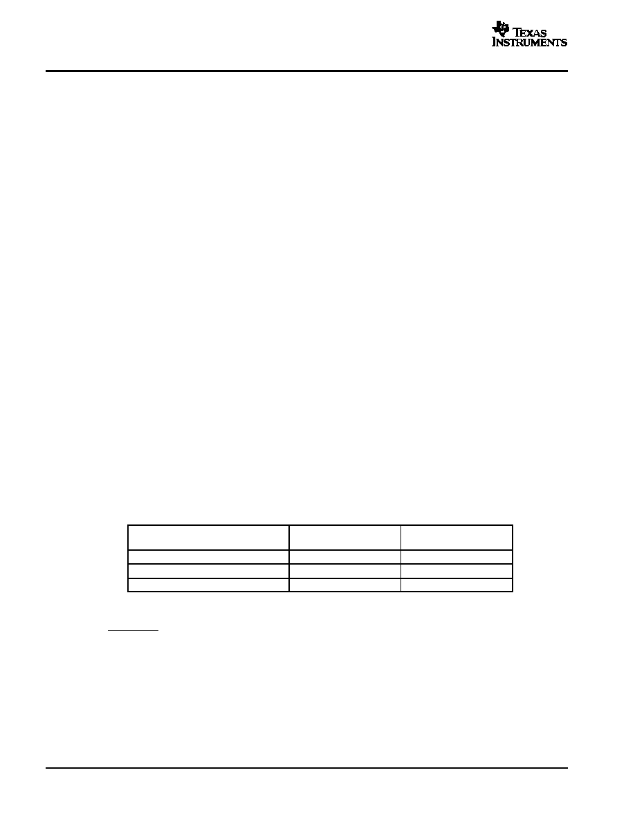
The maximum possible conversion rate per channel is dependent on the selected analog input channels. Table 1
shows the maximum conversion rate for different combinations.
Table 1. Maximum Conversion Rate
CHANNEL CONFIGURATION
NUMBER OF CHANNELS
MAXIMUM CONVERSION
RATE PER CHANNEL
1 single-ended channel
1
8 MSPS
2 single-ended channels
2
4 MSPS
1 differential channel
1
8 MSPS
The maximum conversion rate in the continuous conversion mode per channel, fc, is given by:
fc
+ 8 MSPS
# channels
相关PDF资料 |
PDF描述 |
|---|---|
| THS1209IDAG4 | 2-CH 12-BIT PROPRIETARY METHOD ADC, PARALLEL ACCESS, PDSO32 |
| THS1215CDWRG4 | 1-CH 12-BIT PROPRIETARY METHOD ADC, PARALLEL ACCESS, PDSO28 |
| THS1215IDWRG4 | 1-CH 12-BIT PROPRIETARY METHOD ADC, PARALLEL ACCESS, PDSO28 |
| THS1215CPWRG4 | 1-CH 12-BIT PROPRIETARY METHOD ADC, PARALLEL ACCESS, PDSO28 |
| THS1215CDW | 1-CH 12-BIT PROPRIETARY METHOD ADC, PARALLEL ACCESS, PDSO28 |
相关代理商/技术参数 |
参数描述 |
|---|---|
| THS1209IDA | 功能描述:模数转换器 - ADC 12 Bit 8 MSPS Dual Ch RoHS:否 制造商:Texas Instruments 通道数量:2 结构:Sigma-Delta 转换速率:125 SPs to 8 KSPs 分辨率:24 bit 输入类型:Differential 信噪比:107 dB 接口类型:SPI 工作电源电压:1.7 V to 3.6 V, 2.7 V to 5.25 V 最大工作温度:+ 85 C 安装风格:SMD/SMT 封装 / 箱体:VQFN-32 |
| THS1209IDAG4 | 功能描述:模数转换器 - ADC 12 Bit 8 MSPS Dual Ch RoHS:否 制造商:Texas Instruments 通道数量:2 结构:Sigma-Delta 转换速率:125 SPs to 8 KSPs 分辨率:24 bit 输入类型:Differential 信噪比:107 dB 接口类型:SPI 工作电源电压:1.7 V to 3.6 V, 2.7 V to 5.25 V 最大工作温度:+ 85 C 安装风格:SMD/SMT 封装 / 箱体:VQFN-32 |
| THS121 | 制造商:TOSHIBA 制造商全称:Toshiba Semiconductor 功能描述:HIGH STABILITY MOTOR CONTROL. DIGITAL TACHOMETER. CRANK SHAFT POSITION SENSOR. |
| THS1215 | 制造商:TI 制造商全称:Texas Instruments 功能描述:3.3-V, 12-BIT, 15 MSPS, LOW-POWER ANALOG-TO-DIGITAL CONVERTER WITH POWER DOWN |
| THS1215CDW | 功能描述:模数转换器 - ADC 12-Bit 15 MSPS w/Low Pwr & exc ENOB RoHS:否 制造商:Texas Instruments 通道数量:2 结构:Sigma-Delta 转换速率:125 SPs to 8 KSPs 分辨率:24 bit 输入类型:Differential 信噪比:107 dB 接口类型:SPI 工作电源电压:1.7 V to 3.6 V, 2.7 V to 5.25 V 最大工作温度:+ 85 C 安装风格:SMD/SMT 封装 / 箱体:VQFN-32 |
发布紧急采购,3分钟左右您将得到回复。