参数资料
| 型号: | OP270EZ |
| 厂商: | Analog Devices Inc |
| 文件页数: | 9/20页 |
| 文件大小: | 0K |
| 描述: | IC OPAMP GP 5MHZ DUAL PREC 8CDIP |
| 标准包装: | 48 |
| 放大器类型: | 通用 |
| 电路数: | 2 |
| 转换速率: | 2.4 V/µs |
| 增益带宽积: | 5MHz |
| 电流 - 输入偏压: | 5nA |
| 电压 - 输入偏移: | 10µV |
| 电流 - 电源: | 4mA |
| 电压 - 电源,单路/双路(±): | ±4.5 V ~ 18 V |
| 工作温度: | -40°C ~ 85°C |
| 安装类型: | 通孔 |
| 封装/外壳: | 8-CDIP(0.300",7.62mm) |
| 供应商设备封装: | 8-CERDIP |
| 包装: | 管件 |
| 产品目录页面: | 772 (CN2011-ZH PDF) |
OP270
Rev. E | Page 17 of 20
0
325
-045
1/2
OP270GP
VIN
NC
RFBA
1
23
24
22
18
19
CS
WR
WRITE
CONTROL
20
6
5
7
3
2
4
3
21
VDD
DAC8221P
2
8
4
0.01F
+15V
–15V
OUT
IOUTA
IOUTB
AGND
DGND
5
1/2
OP270GP
DAC B
DAC A
+5V
10F
–
+
10F
–
+
0.1F
RFBB
VREFA
VREFB
DAC A/DAC B
DAC DATA BUS
PINS 6 (MSB) TO 17 (LSB)
OUT
DIGITAL PANNING CONTROL
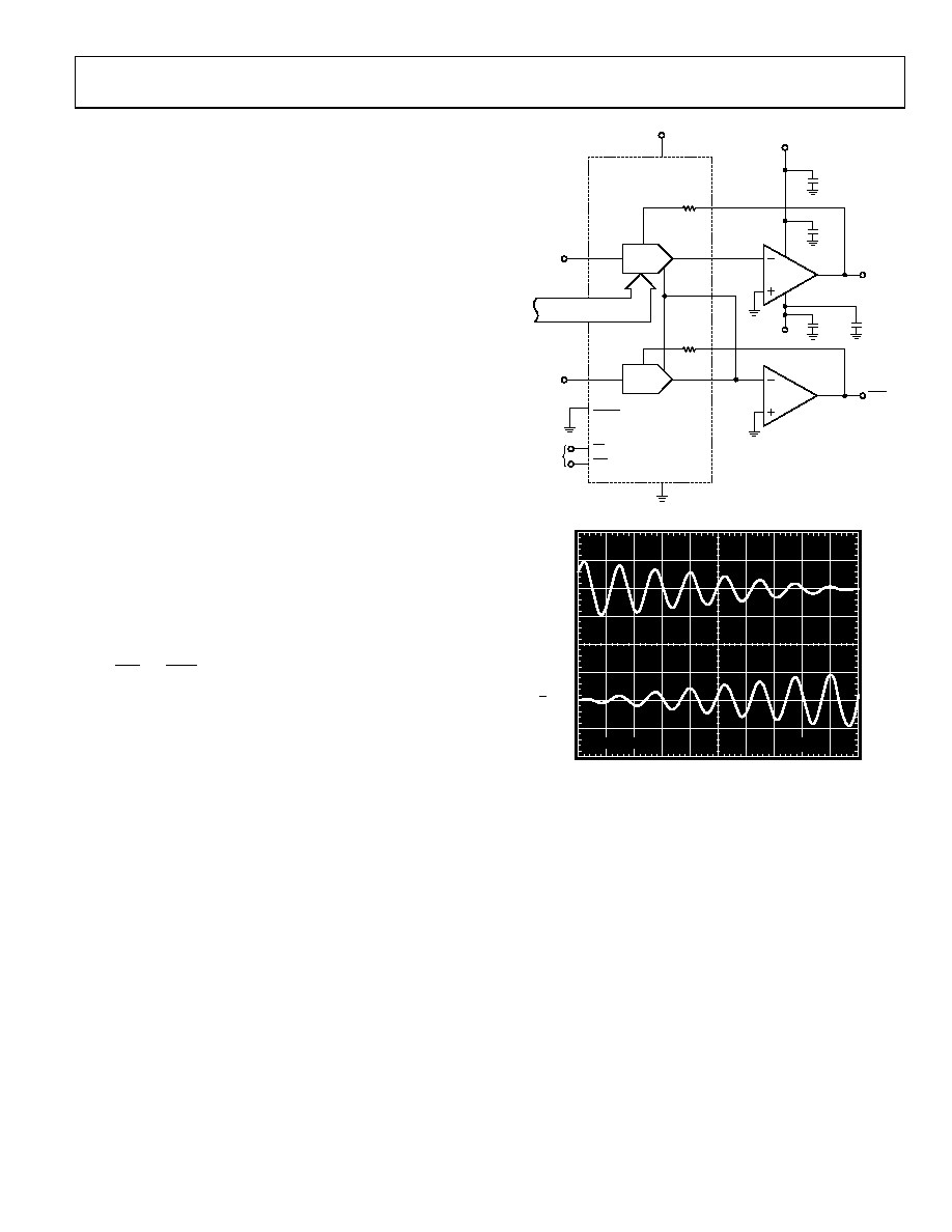
signal between two channels. One channel is formed by the
current output of DAC A driving one-half of an OP270 in a
current-to-voltage converter configuration. The other channel
is formed by the complementary output current of DAC A,
which normally flows to ground through the AGND pin. This
complementary current is converted to a voltage by the other
half of the OP270, which also holds AGND at virtual ground.
Gain error due to mismatching between the internal DAC
ladder resistors and the current-to-voltage feedback resistors is
eliminated by using feedback resistors internal to the DAC8221.
Only DAC A passes a signal; DAC B provides the second
feedback resistor. With VREFB unconnected, the current-to-
voltage converter, using RFBB, is accurate and not influenced by
digital data reaching DAC B. Distortion of the digital panning
control is less than 0.002% over the 20 Hz to 20 kHz audio
range. Figure 45 shows the complementary outputs for a 1 kHz
input signal and a digital ramp applied to the DAC data input.
DUAL PROGRAMMABLE GAIN AMPLIFIER
Figure 44. Digital Panning Control
The dual OP270 and the DAC8221 (a dual 12-bit CMOS DAC)
can be combined to form a space-saving, dual programmable
amplifier. The digital code present at the DAC, which is easily
set by a microprocessor, determines the ratio between the internal
feedback resistor and the resistance that the DAC ladder presents
to the op amp feedback loop. Gain of each amplifier is
00
35
2-
0
46
5V
1ms
A OUT
n
V
IN
O
4096
=
where n is the decimal equivalent of the 12-bit digital code
present at the DAC.
If the digital code present at the DAC consists of all 0s, the
feedback loop opens, causing the op amp output to saturate. A
20 MΩ resistor placed in parallel with the DAC feedback loop
eliminates this problem with only a very small reduction in gain
accuracy.
Figure 45. Digital Panning Control Output
相关PDF资料 |
PDF描述 |
|---|---|
| 929647-09-04-I | CONN HEADER .100 SNGL STR 4POS |
| OP467GSZ | IC OPAMP GP 28MHZ QUAD 16SOIC |
| AD8620ARZ | IC OPAMP JFET 25MHZ DUAL 8SOIC |
| NZQA5V6XV5T1G | TVS ARRAY QUAD ESD 5.6V SOT553 |
| OP400FY | IC OPAMP GP 500KHZ QUAD 14CDIP |
相关代理商/技术参数 |
参数描述 |
|---|---|
| OP-270EZ | 制造商:AD 制造商全称:Analog Devices 功能描述:DUAL VERY LOW NOISE PRECISION OPERATIONAL AMPLIFIER |
| OP270FZ | 功能描述:IC OPAMP GP 5MHZ DUAL PREC 8CDIP RoHS:否 类别:集成电路 (IC) >> Linear - Amplifiers - Instrumentation 系列:- 标准包装:2,500 系列:- 放大器类型:通用 电路数:4 输出类型:- 转换速率:0.6 V/µs 增益带宽积:1MHz -3db带宽:- 电流 - 输入偏压:45nA 电压 - 输入偏移:2000µV 电流 - 电源:1.4mA 电流 - 输出 / 通道:40mA 电压 - 电源,单路/双路(±):3 V ~ 32 V,±1.5 V ~ 16 V 工作温度:0°C ~ 70°C 安装类型:表面贴装 封装/外壳:14-TSSOP(0.173",4.40mm 宽) 供应商设备封装:14-TSSOP 包装:带卷 (TR) 其它名称:LM324ADTBR2G-NDLM324ADTBR2GOSTR |
| OP-270FZ | 制造商:AD 制造商全称:Analog Devices 功能描述:DUAL VERY LOW NOISE PRECISION OPERATIONAL AMPLIFIER |
| OP-270G | 制造商:LINER 制造商全称:Linear Technology 功能描述:Dual/Quad Low Noise, Precision Operational Amplifiers |
| OP270GBC | 制造商:未知厂家 制造商全称:未知厂家 功能描述:Voltage-Feedback Operational Amplifier |
发布紧急采购,3分钟左右您将得到回复。