- 您现在的位置:买卖IC网 > PDF目录4041 > MPC8567EVTAUJJ (Freescale Semiconductor)MPU POWERQUICC III 1023-PBGA PDF资料下载
参数资料
| 型号: | MPC8567EVTAUJJ |
| 厂商: | Freescale Semiconductor |
| 文件页数: | 35/139页 |
| 文件大小: | 0K |
| 描述: | MPU POWERQUICC III 1023-PBGA |
| 标准包装: | 24 |
| 系列: | MPC85xx |
| 处理器类型: | 32-位 MPC85xx PowerQUICC III |
| 速度: | 1.333GHz |
| 电压: | 1.1V |
| 安装类型: | 表面贴装 |
| 封装/外壳: | 1023-BBGA,FCBGA |
| 供应商设备封装: | 1023-FCPBGA(33x33) |
| 包装: | 托盘 |
第1页第2页第3页第4页第5页第6页第7页第8页第9页第10页第11页第12页第13页第14页第15页第16页第17页第18页第19页第20页第21页第22页第23页第24页第25页第26页第27页第28页第29页第30页第31页第32页第33页第34页当前第35页第36页第37页第38页第39页第40页第41页第42页第43页第44页第45页第46页第47页第48页第49页第50页第51页第52页第53页第54页第55页第56页第57页第58页第59页第60页第61页第62页第63页第64页第65页第66页第67页第68页第69页第70页第71页第72页第73页第74页第75页第76页第77页第78页第79页第80页第81页第82页第83页第84页第85页第86页第87页第88页第89页第90页第91页第92页第93页第94页第95页第96页第97页第98页第99页第100页第101页第102页第103页第104页第105页第106页第107页第108页第109页第110页第111页第112页第113页第114页第115页第116页第117页第118页第119页第120页第121页第122页第123页第124页第125页第126页第127页第128页第129页第130页第131页第132页第133页第134页第135页第136页第137页第138页第139页
MPC8568E/MPC8567E PowerQUICC III Integrated Processor Hardware Specifications, Rev. 1
Freescale Semiconductor
13
Electrical Characteristics
The core voltage must always be provided at nominal 1.1V. (See Table 3 for actual recommended core
voltage). Voltage to the processor interface I/Os are provided through separate sets of supply pins and must
be provided at the voltages shown in Table 3. The input voltage threshold scales with respect to the
associated I/O supply voltage. OVDD and LVDD based receivers are simple CMOS I/O circuits and satisfy
appropriate LVCMOS type specifications. The DDR SDRAM interface uses a single-ended differential
receiver referenced the externally supplied MVREF signal (nominally set to GVDD/2) as is appropriate for
the SSTL2 electrical signaling standard.
2.1.3
Output Driver Characteristics
Table 4 provides information on the characteristics of the output driver strengths. The values are
preliminary estimates.
2.2
Power Sequencing
The MPC8568E requires its power rails to be applied in specific sequence in order to ensure proper device
operation. These requirements are as follows for power up:
1. VDD, AVDD_n, BVDD, SCOREVDD, LVDD, TVDD, XVDD, OVDD
2. GVDD
All supplies must be at their stable values within 50 ms.
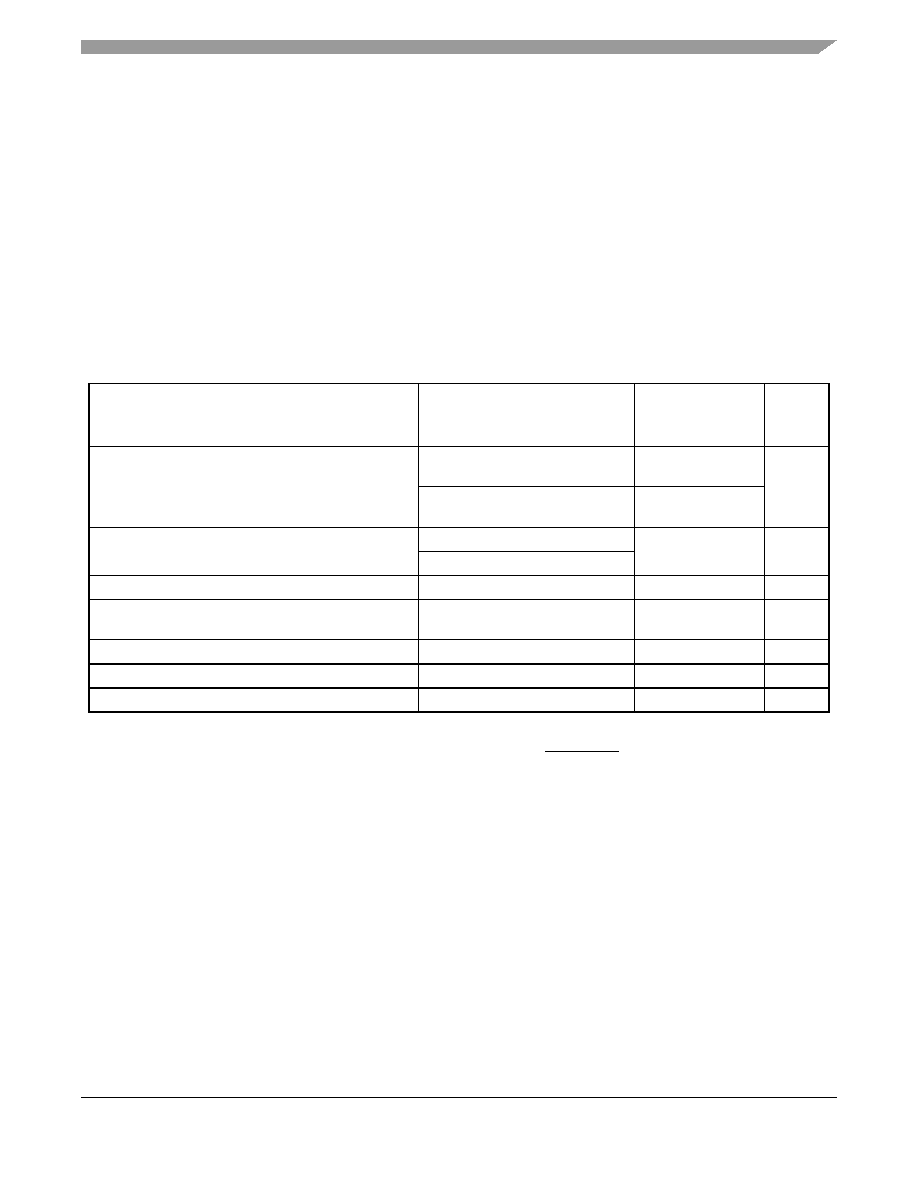
Table 4. Output Drive Capability
Driver Type
Programmable
Output Impedance
(
Ω)
Supply
Voltage
Notes
Local bus interface utilities signals
25
BVDD = 3.3 V
BVDD = 2.5 V
1
45(default)
BVDD = 3.3 V
BVDD = 2.5 V
PCI signals
25
OVDD = 3.3 V
2
42 (default)
DDR signal
20
GVDD = 2.5 V
—
DDR2 signal
16
32 (half strength mode)
GVDD = 1.8 V
—
eTSEC 10/100/1000 signals
42
L/TVDD = 2.5/3.3 V
—
DUART, system control, JTAG
42
OVDD = 3.3 V
—
I2C
150
OVDD = 3.3 V
—
Notes:
1. The drive strength of the local bus interface is determined by the configuration of the appropriate bits in PORIMPSCR.
2. The drive strength of the PCI interface is determined by the setting of the PCI_GNT[1] signal at reset.
相关PDF资料 |
PDF描述 |
|---|---|
| IDT70V9359L9BF | IC SRAM 144KBIT 9NS 100FBGA |
| MC68LC040RC33A | IC MPU 32BIT 33MHZ 179-PGA |
| MC7447AVU1267LB | IC MPU RISC 32BIT 360-BGA |
| ASC17DTEF | CONN EDGECARD 34POS .100 EYELET |
| IDT70V9169L9BF | IC SRAM 144KBIT 9NS 100FBGA |
相关代理商/技术参数 |
参数描述 |
|---|---|
| MPC8567VTANGG | 功能描述:微处理器 - MPU 800MHz Non-Encrypt RoHS:否 制造商:Atmel 处理器系列:SAMA5D31 核心:ARM Cortex A5 数据总线宽度:32 bit 最大时钟频率:536 MHz 程序存储器大小:32 KB 数据 RAM 大小:128 KB 接口类型:CAN, Ethernet, LIN, SPI,TWI, UART, USB 工作电源电压:1.8 V to 3.3 V 最大工作温度:+ 85 C 安装风格:SMD/SMT 封装 / 箱体:FBGA-324 |
| MPC8567VTAQGG | 功能描述:微处理器 - MPU 1GHz Non-Encrypt RoHS:否 制造商:Atmel 处理器系列:SAMA5D31 核心:ARM Cortex A5 数据总线宽度:32 bit 最大时钟频率:536 MHz 程序存储器大小:32 KB 数据 RAM 大小:128 KB 接口类型:CAN, Ethernet, LIN, SPI,TWI, UART, USB 工作电源电压:1.8 V to 3.3 V 最大工作温度:+ 85 C 安装风格:SMD/SMT 封装 / 箱体:FBGA-324 |
| MPC8567VTAUJJ | 功能描述:微处理器 - MPU Non-Encrypt No PB 1.3GHz RoHS:否 制造商:Atmel 处理器系列:SAMA5D31 核心:ARM Cortex A5 数据总线宽度:32 bit 最大时钟频率:536 MHz 程序存储器大小:32 KB 数据 RAM 大小:128 KB 接口类型:CAN, Ethernet, LIN, SPI,TWI, UART, USB 工作电源电压:1.8 V to 3.3 V 最大工作温度:+ 85 C 安装风格:SMD/SMT 封装 / 箱体:FBGA-324 |
| MPC8568ECVTAQGG | 功能描述:微处理器 - MPU 8568 1GHz Pb Free RoHS:否 制造商:Atmel 处理器系列:SAMA5D31 核心:ARM Cortex A5 数据总线宽度:32 bit 最大时钟频率:536 MHz 程序存储器大小:32 KB 数据 RAM 大小:128 KB 接口类型:CAN, Ethernet, LIN, SPI,TWI, UART, USB 工作电源电压:1.8 V to 3.3 V 最大工作温度:+ 85 C 安装风格:SMD/SMT 封装 / 箱体:FBGA-324 |
| MPC8568E-MDS-PB | 功能描述:开发板和工具包 - 其他处理器 MPC8568E FAMILY ADS RoHS:否 制造商:Freescale Semiconductor 产品:Development Systems 工具用于评估:P3041 核心:e500mc 接口类型:I2C, SPI, USB 工作电源电压: |
发布紧急采购,3分钟左右您将得到回复。