参数资料
| 型号: | MC74HCT273AN |
| 厂商: | ON Semiconductor |
| 文件页数: | 2/7页 |
| 文件大小: | 0K |
| 描述: | IC FLIP FLOP OCT CLK/RST 20DIP |
| 产品变化通告: | Product Discontinuation 20/Aug/2008 |
| 标准包装: | 18 |
| 系列: | 74HCT |
| 功能: | 复位 |
| 类型: | D 型总线 |
| 输出类型: | 非反相 |
| 元件数: | 1 |
| 每个元件的位元数: | 8 |
| 频率 - 时钟: | 30MHz |
| 延迟时间 - 传输: | 25ns |
| 触发器类型: | 正边沿 |
| 输出电流高,低: | 4mA,4mA |
| 电源电压: | 4.5 V ~ 5.5 V |
| 工作温度: | -55°C ~ 125°C |
| 安装类型: | 通孔 |
| 封装/外壳: | 20-DIP(0.300",7.62mm) |
| 包装: | 管件 |
| 其它名称: | MC74HCT273ANOS |
MC74HCT273A
http://onsemi.com
2
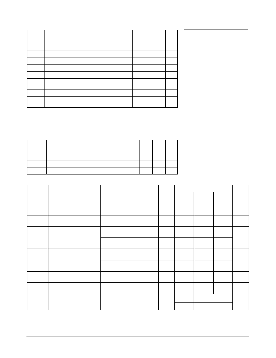
MAXIMUM RATINGS
Symbol
Parameter
Value
Unit
VCC
DC Supply Voltage (Referenced to GND)
– 0.5 to + 7.0
V
Vin
DC Input Voltage (Referenced to GND)
– 0.5 to VCC + 0.5
V
Vout
DC Output Voltage (Referenced to GND)
– 0.5 to VCC + 0.5
V
Iin
DC Input Current, per Pin
± 20
mA
Iout
DC Output Current, per Pin
± 25
mA
ICC
DC Supply Current, VCC and GND Pins
± 50
mA
PD
Power Dissipation in Still Air
PDIP
SOIC Package
750
500
mW
Tstg
Storage Temperature
– 65 to + 150
_C
TL
Lead Temperature, 1 mm from Case for 10 Seconds
(SOIC or PDIP)
260
_C
Stresses exceeding Maximum Ratings may damage the device. Maximum Ratings are stress ratings only. Functional operation above
the Recommended Operating Conditions is not implied. Extended exposure to stresses above the Recommended Operating Conditions
may affect device reliability.
Derating — Plastic DIP: – 10 mW/_C from 65_ to 125_C
SOIC Package: – 7 mW/_C from 65_ to 125_C
RECOMMENDED OPERATING CONDITIONS
Symbol
Parameter
Min
Max
Unit
VCC
DC Supply Voltage (Referenced to GND)
4.5
5.5
V
Vin, Vout
DC Input Voltage, Output Voltage (Referenced to GND)
0
VCC
V
TA
Operating Temperature, All Package Types
– 55
+ 125
_C
tr, tf
Input Rise and Fall Time (Figure 1)
0
500
ns
DC ELECTRICAL CHARACTERISTICS (Voltages Referenced to GND)
Symbol
Parameter
Test Conditions
VCC
V
Guaranteed Limit
Unit
– 55 to
25_C
v 85_C
v 125_C
VIH
Minimum HighLevel Input
Voltage
Vout = 0.1 V or VCC – 0.1 V
|Iout| v 20 μA
4.5
5.5
2.0
2.0
2.0
V
VIL
Maximum LowLevel Input
Voltage
Vout = 0.1 V or VCC – 0.1 V
|Iout| v 20 μA
4.5
5.5
0.8
0.8
0.8
V
VOH
Minimum HighLevel Output
Voltage
Vin = VIH or VIL
|Iout| v 20 μA
4.5
5.5
4.4
5.4
4.4
5.4
4.4
5.4
V
Vin = VIH or VIL
|Iout| v 4.0 mA
4.5
3.98
3.84
3.7
VOL
Maximum LowLevel Output
Voltage
Vin = VIH or VIL
|Iout| v 20 μA
4.5
5.5
0.1
0.1
0.1
V
Vin = VIH or VIL
|Iout| v 4.0 mA
4.5
0.26
0.33
0.4
Iin
Maximum Input Leakage Cur-
rent
Vin = VCC or GND
5.5
± 0.1
± 1.0
± 1.0
μA
ICC
Maximum Quiescent Supply
Current (per Package)
Vin = VCC or GND
Iout = 0 μA
5.5
4.0
40
160
μA
ΔICC
Additional Quiescent Supply
Current
Vin = 2.4 V, Any One Input
Vin = VCC or GND, Other Inputs
lout = 0 μA
5.5
≥ 55_C
25_C to 125_C
mA
2.9
2.4
This device contains protection
circuitry to guard against damage
due to high static voltages or electric
fields. However, precautions must
be taken to avoid applications of any
voltage higher than maximum rated
voltages to this highimpedance cir-
cuit. For proper operation, Vin and
Vout should be constrained to the
range GND v (Vin or Vout) v VCC.
Unused inputs must always be
tied to an appropriate logic voltage
level (e.g., either GND or VCC).
Unused outputs must be left open.
相关PDF资料 |
PDF描述 |
|---|---|
| MC74HCT74AN | IC FLIP FLOP DUAL SET/RST 14DIP |
| MC74HC175AN | IC FLIP FLOP QUAD CLK/RST 16DIP |
| MC14013BDR2 | IC FLIP-FLOP DUAL CMOS 14SOIC |
| 2544000 | FUSEBLOCK 3POLE 10MMX38MM DNRAIL |
| 74AHCT241BQ,115 | IC BUFFER/LINEDVR 3ST DHVQFN20 |
相关代理商/技术参数 |
参数描述 |
|---|---|
| MC74HCT273ANG | 功能描述:触发器 5V CMOS Octal D-Type RoHS:否 制造商:Texas Instruments 电路数量:2 逻辑系列:SN74 逻辑类型:D-Type Flip-Flop 极性:Inverting, Non-Inverting 输入类型:CMOS 输出类型: 传播延迟时间:4.4 ns 高电平输出电流:- 16 mA 低电平输出电流:16 mA 电源电压-最大:5.5 V 最大工作温度:+ 85 C 安装风格:SMD/SMT 封装 / 箱体:X2SON-8 封装:Reel |
| MC74HCT273N | 制造商:Freescale Semiconductor 功能描述: |
| MC74HCT32AD | 制造商:Rochester Electronics LLC 功能描述:- Bulk |
| MC74HCT32ADG | 功能描述:逻辑门 QUAD 2-I OR GATE W/LSTTL RoHS:否 制造商:Texas Instruments 产品:OR 逻辑系列:LVC 栅极数量:2 线路数量(输入/输出):2 / 1 高电平输出电流:- 16 mA 低电平输出电流:16 mA 传播延迟时间:3.8 ns 电源电压-最大:5.5 V 电源电压-最小:1.65 V 最大工作温度:+ 125 C 安装风格:SMD/SMT 封装 / 箱体:DCU-8 封装:Reel |
| MC74HCT32ADR2 | 制造商:ON Semiconductor 功能描述:OR Gate 4-Element 2-IN CMOS 14-Pin SOIC N T/R 制造商:Rochester Electronics LLC 功能描述:- Bulk |
发布紧急采购,3分钟左右您将得到回复。