- 您现在的位置:买卖IC网 > PDF目录5516 > MAX4223ESA+T (Maxim Integrated Products)IC AMP CURRENT FB LP 8-SOIC PDF资料下载
参数资料
| 型号: | MAX4223ESA+T |
| 厂商: | Maxim Integrated Products |
| 文件页数: | 4/20页 |
| 文件大小: | 0K |
| 描述: | IC AMP CURRENT FB LP 8-SOIC |
| 产品培训模块: | Lead (SnPb) Finish for COTS Obsolescence Mitigation Program |
| 标准包装: | 2,500 |
| 放大器类型: | 电流反馈 |
| 电路数: | 1 |
| 转换速率: | 1100 V/µs |
| -3db带宽: | 1GHz |
| 电流 - 输入偏压: | 4µA |
| 电压 - 输入偏移: | 500µV |
| 电流 - 电源: | 6mA |
| 电流 - 输出 / 通道: | 80mA |
| 电压 - 电源,单路/双路(±): | ±2.85 V ~ 5.5 V |
| 工作温度: | -40°C ~ 85°C |
| 安装类型: | 表面贴装 |
| 封装/外壳: | 8-SOIC(0.154",3.90mm 宽) |
| 供应商设备封装: | 8-SOIC |
| 包装: | 带卷 (TR) |
MAX4223–MAX4228
1GHz, Low-Power, SOT23,
Current-Feedback Amplifiers with Shutdown
12
______________________________________________________________________________________
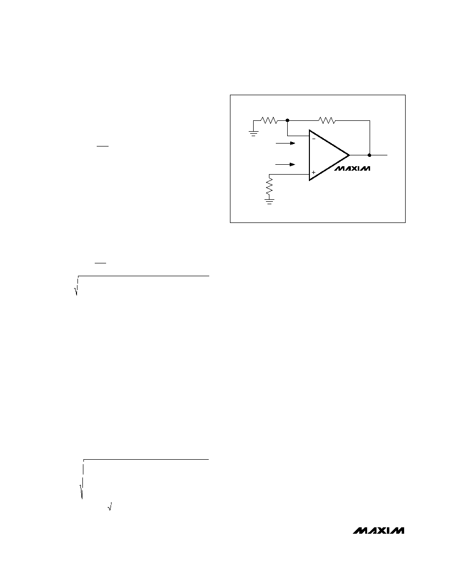
DC and Noise Errors
The MAX4223–MAX4228 output offset voltage, VOUT
(Figure 2), can be calculated with the following equation:
where:
VOS = input offset voltage (in volts)
1 + RF / RG = amplifier closed-loop gain (dimensionless)
IB+ = input bias current (in amps)
IB- = inverting input bias current (in amps)
RG = gain-setting resistor (in
)
RF = feedback resistor (in
)
RS = source resistor (in
)
The following equation represents output noise density:
where:
in = input noise current density (in pA/
√Hz)
en = input noise voltage density (in nV/
√Hz)
The MAX4223–MAX4228 have a very low, 2nV/
√Hz
noise voltage. The current noise at the noninverting
input (in+) is 3pA/
√Hz, and the current noise at the
inverting input (in-) is 20pA/
√Hz.
An example of DC-error calculations, using the
MAX4224 typical data and the typical operating circuit
with RF = RG = 470
(RF || RG = 235) and RS = 50,
gives:
VOUT = [5 x 10-4 x (1 + 1)] + [2 x 10-6 x 50 x (1 + 1)] +
[4 x 10-6 x 470]
VOUT = 3.1mV
Calculating total output noise in a similar manner yields
the following:
With a 600MHz system bandwidth, this calculates to
250VRMS (approximately 1.5mVp-p, using the six-
sigma calculation).
Communication Systems
Nonlinearities of components used in a communication
system produce distortion of the desired output signal.
Intermodulation distortion (IMD) is the distortion that
results from the mixing of two input signals of different
frequencies in a nonlinear system. In addition to the
input signal frequencies, the resulting output signal
contains new frequency components that represent the
sum and difference products of the two input frequen-
cies. If the two input signals are relatively close in fre-
quency, the third-order sum and difference products
will fall close to the frequency of the desired output and
will therefore be very difficult to filter. The third-order
intercept (IP3) is defined as the power level at which
the amplitude of the largest third-order product is equal
to the power level of the desired output signal. Higher
third-order intercept points correspond to better lineari-
ty of the amplifier. The MAX4223–MAX4228 have a typi-
cal IP3 value of 42dBm, making them excellent choices
for use in communications systems.
ADC Input Buffers
Input buffer amplifiers can be a source of significant
errors in high-speed ADC applications. The input buffer
is usually required to rapidly charge and discharge the
ADC’s input, which is often capacitive (see the section
Driving Capacitive Loads). In addition, a high-speed
ADC’s input impedance often changes very rapidly
during the conversion cycle, requiring an amplifier with
e
x
e
nV
Hz
n OUT
( )
( )
=
+
(
)
+
+
=
.
/
1
3
10
50
20
10
235
2
10
10 2
12
2
9
2
e
R
x
i
x R
i
x R
R
e
n OUT
F
G
n
S
n
F
G
n
( )
+
=
+
(
) +
(
)
[
] +( )
||
1
2
V
x 1
R /R
I
x R
x 1
R
I
x R
OUT
OS
F
G
B
S
F
G
B
F
=
+
(
) +
+
+
MAX4223
MAX4224
MAX4225
MAX4226
MAX4227
MAX4228
RG
IN-
IB-
IB+
IN+
VOUT
OUT
RS
RF
Figure 2. Output Offset Voltage
相关PDF资料 |
PDF描述 |
|---|---|
| 6648056-1 | CONN,SKT |
| 320571 | CONN RING 16-22 AWG #1/4 PIDG |
| LPSJ301.ZXID | FUSEHOLDER CLASS J 30A 1POLE |
| 31894 | CONN RING 16-22 AWG #1/4 PIDG |
| MAX9633ATA+T | IC OPAMP GP 27MHZ LN 8TDFN |
相关代理商/技术参数 |
参数描述 |
|---|---|
| MAX4223EUT | 制造商:Maxim Integrated Products 功能描述:NON BOOK, REQUIRES Q#, NC/NR - Cut Tape Product |
| MAX4223EUT+ | 制造商:Maxim Integrated Products 功能描述:OP AMP SGL CURRENT FDBK 5.5V 6PIN SOT-23 - Rail/Tube |
| MAX4223EUT+T | 功能描述:高速运算放大器 1GHz Current Feedback Amp RoHS:否 制造商:Texas Instruments 通道数量:1 电压增益 dB:116 dB 输入补偿电压:0.5 mV 转换速度:55 V/us 工作电源电压:36 V 电源电流:7.5 mA 最大工作温度:+ 85 C 安装风格:SMD/SMT 封装 / 箱体:SOIC-8 封装:Tube |
| MAX4223EUT-T | 功能描述:高速运算放大器 Integrated Circuits (ICs) RoHS:否 制造商:Texas Instruments 通道数量:1 电压增益 dB:116 dB 输入补偿电压:0.5 mV 转换速度:55 V/us 工作电源电压:36 V 电源电流:7.5 mA 最大工作温度:+ 85 C 安装风格:SMD/SMT 封装 / 箱体:SOIC-8 封装:Tube |
| MAX4223EVKIT | 功能描述:高速运算放大器 Programmers, Development Systems RoHS:否 制造商:Texas Instruments 通道数量:1 电压增益 dB:116 dB 输入补偿电压:0.5 mV 转换速度:55 V/us 工作电源电压:36 V 电源电流:7.5 mA 最大工作温度:+ 85 C 安装风格:SMD/SMT 封装 / 箱体:SOIC-8 封装:Tube |
发布紧急采购,3分钟左右您将得到回复。