参数资料
| 型号: | LTC6410CUD-6#TRPBF |
| 厂商: | Linear Technology |
| 文件页数: | 2/16页 |
| 文件大小: | 0K |
| 描述: | IC AMP DIFF IF 16-QFN |
| 标准包装: | 2,500 |
| 放大器类型: | 差分 |
| 电路数: | 1 |
| 输出类型: | 差分 |
| 转换速率: | 1500 V/µs |
| -3db带宽: | 1.4GHz |
| 电压 - 输入偏移: | 400µV |
| 电流 - 电源: | 125mA |
| 电流 - 输出 / 通道: | 42mA |
| 电压 - 电源,单路/双路(±): | 2.8 V ~ 5.5 V,±1.4 V ~ 2.75 V |
| 工作温度: | 0°C ~ 70°C |
| 安装类型: | 表面贴装 |
| 封装/外壳: | 16-WFQFN 裸露焊盘 |
| 供应商设备封装: | 16-QFN-EP(3x3) |
| 包装: | 带卷 (TR) |
LTC6410-6
10
64106fa
PIN FUNCTIONS
V– (Pins 1, 4, 9, 12, 17): Negative Power Supply (Normally
Tied to Ground). All 5 pins must be tied to the same voltage.
V– maybe tied to a voltage other than ground as long as the
voltage between V+ and V– is 2.8V to 5.5V. If the V– pins
are not tied to ground, bypass each with 680pF and 0.1μF
capacitors as close to the package as possible.
VBIAS (Pin 2): This pin sets the input and output com-
mon mode voltage by driving the +IN and –IN through a
buffer with a high output resistance of 1k. If the part is
AC-coupled at the input, the VBIAS will set the VINCM and
therefore the VOUTCM voltage. If the part is DC-coupled at
the input, VBIAS should be left oating. Internal resistors
bias VBIAS to 1.4V on a 3V supply.
V+ (Pins 3, 5, 8, 10):
Positive Power Supply. All 4 pins
must be tied to the same voltage. Split supplies are pos-
sible as long as the voltage between V+ and V– is 2.8V to
5.5V. Bypass capacitors of 680pF and 0.1μF as close to the
part as possible should be used between supplies.
+OUT, –OUT (Pins 6, 7): Outputs. These pins each have
internal series termination resistors forming a differential
output resistance.
SHDN (Pin 11): This pin is internally pulled high by a typi-
cally 30k resistor to V+. By pulling this pin low the supply
current will be reduced to typically 3mA. See DC Electrical
Characteristics table for the specic logic levels.
–TERM (Pin 13): Negative Input Termination. When tied
directly to –IN, it provides an active 50Ω differential ter-
mination when +TERM is also tied directly to +IN.
–IN (Pin 14): Negative Input. This pin is normally tied to
–TERM, the input termination pin. If AC-coupled, this pin
will self bias by VBIAS.
+IN (Pin 15): Positive Input. This pin is normally tied to
+TERM, the input termination pin. If AC-coupled, this pin
will self bias by VBIAS.
+TERM (Pin 16): Positive Input Termination. When tied
directly to +IN, it provides an active 50Ω differential ter-
mination when –TERM is also tied directly to –IN.
Exposed Pad (Pin 17): V–. The Exposed Pad must be
soldered to the PCB metal.
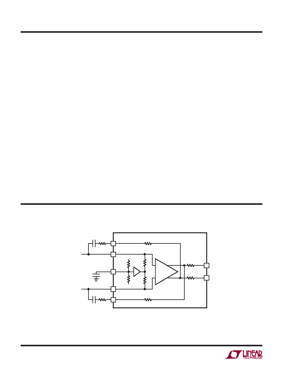
BLOCK DIAGRAM
64106 BD
–IN
+IN
1k
6.4k
V+
V–
VBIAS
REXT
(OPT)
REXT
(OPT)
CEXT
(OPT)
CEXT
(OPT)
RO
11Ω
RO
11Ω
–OUT
+OUT
5.7k
RT
110Ω
RT
110Ω
+
–
+
–
+TERM
–IN
+IN
0.1μF
–TERM
+1
AV = 2.7V/V
相关PDF资料 |
PDF描述 |
|---|---|
| SSQ-110-02-G-S-RA | CONN RCPT .100" 10POS R/A SGL AU |
| HPC12JT22R0 | RES 22 OHM 5W 5% SMD |
| RMCF0805FT2K43 | RES 2.43K OHM 1/8W 1% 0805 SMD |
| 776087-5 | 23 POS AMPSEAL HDR SNAP IN W/G |
| TSW-139-26-G-S | CONN HEADER 39POS .100" SGL GOLD |
相关代理商/技术参数 |
参数描述 |
|---|---|
| LTC6410IUD-6#PBF | 功能描述:IC AMP DIFF IF 16-QFN RoHS:是 类别:集成电路 (IC) >> Linear - Amplifiers - Instrumentation 系列:- 标准包装:1 系列:- 放大器类型:通用 电路数:4 输出类型:满摆幅 转换速率:0.028 V/µs 增益带宽积:105kHz -3db带宽:- 电流 - 输入偏压:3nA 电压 - 输入偏移:100µV 电流 - 电源:3.3µA 电流 - 输出 / 通道:12mA 电压 - 电源,单路/双路(±):2.7 V ~ 12 V,±1.35 V ~ 6 V 工作温度:-40°C ~ 85°C 安装类型:表面贴装 封装/外壳:14-TSSOP(0.173",4.40mm 宽) 供应商设备封装:14-TSSOP 包装:剪切带 (CT) 其它名称:OP481GRUZ-REELCT |
| LTC6410IUD-6#TRPBF | 功能描述:IC AMP DIFF IF 16-QFN RoHS:是 类别:集成电路 (IC) >> Linear - Amplifiers - Instrumentation 系列:- 标准包装:1 系列:- 放大器类型:通用 电路数:4 输出类型:满摆幅 转换速率:0.028 V/µs 增益带宽积:105kHz -3db带宽:- 电流 - 输入偏压:3nA 电压 - 输入偏移:100µV 电流 - 电源:3.3µA 电流 - 输出 / 通道:12mA 电压 - 电源,单路/双路(±):2.7 V ~ 12 V,±1.35 V ~ 6 V 工作温度:-40°C ~ 85°C 安装类型:表面贴装 封装/外壳:14-TSSOP(0.173",4.40mm 宽) 供应商设备封装:14-TSSOP 包装:剪切带 (CT) 其它名称:OP481GRUZ-REELCT |
| LTC6410IUD-6-PBF | 制造商:LINER 制造商全称:Linear Technology 功能描述:Low Distortion, Low Noise Differential IF Amplifi er with Confi gurable Input Impedance |
| LTC6410IUD-6-TRPBF | 制造商:LINER 制造商全称:Linear Technology 功能描述:Low Distortion, Low Noise Differential IF Amplifi er with Confi gurable Input Impedance |
| LTC6411 | 制造商:LINER 制造商全称:Linear Technology 功能描述:2.7GHz, 5V, Low Noise,Rail-to-Rail Input Differential Amplifier/Driver |
发布紧急采购,3分钟左右您将得到回复。