参数资料
| 型号: | LTC6241HVCS8#TRPBF |
| 厂商: | Linear Technology |
| 文件页数: | 16/32页 |
| 文件大小: | 0K |
| 描述: | IC OP AMP DUAL R-R 8-SOIC |
| 标准包装: | 2,500 |
| 放大器类型: | 通用 |
| 电路数: | 2 |
| 输出类型: | 满摆幅 |
| 转换速率: | 10 V/µs |
| 增益带宽积: | 18MHz |
| 电流 - 输入偏压: | 0.5pA |
| 电压 - 输入偏移: | 50µV |
| 电流 - 电源: | 2.5mA |
| 电流 - 输出 / 通道: | 35mA |
| 电压 - 电源,单路/双路(±): | 2.8 V ~ 11 V,±1.4 V ~ 5.5 V |
| 工作温度: | 0°C ~ 70°C |
| 安装类型: | 表面贴装 |
| 封装/外壳: | 8-SOIC(0.154",3.90mm 宽) |
| 供应商设备封装: | 8-SO |
| 包装: | 带卷 (TR) |
第1页第2页第3页第4页第5页第6页第7页第8页第9页第10页第11页第12页第13页第14页第15页当前第16页第17页第18页第19页第20页第21页第22页第23页第24页第25页第26页第27页第28页第29页第30页第31页第32页
LTC6240/LTC6241/LTC6242
23
624012fe
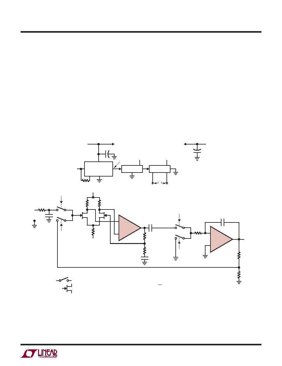
Figure 9. Ultralow Noise Chopper Amplier
to achieve an extraordinarily low noise and low DC drift.
The performance of this circuit is suited for the demand-
ing transducer signal conditioning situations such as high
resolution scales and magnetic search coils.
The LTC1799’s output is divided down to form a 2-phase
925Hz square wave clock. This frequency, harmonically
unrelated to 60Hz, provides excellent immunity to harmonic
beating or mixing effects which could cause instabilities.
S1 and S2 receive complementary drive, causing A1 to
see a chopped version of the input voltage. A1’s square
wave output is synchronously demodulated by S3 and
S4. Because these switches are synchronously driven
with the input chopper, proper amplitude and polarity
information is presented to A2, the DC output amplier.
This stage integrates the square wave into a DC voltage,
providing the output. The output is divided down (R2 and
R1) and fed back to the input chopper where it serves as
a zero signal reference. Gain, in this case 1000, is set by
the R1-R2 ratio. Because A1 is AC coupled, its DC offset
and drift do not affect the overall circuit offset, resulting
in the extremely low offset and drift noted. The JFETs
have an input RC damper that minimizes offset voltage
contribution due to parasitic switch behavior, resulting in
the 1μV offset specication.
APPLICATIONS INFORMATION
+
–
+
–
BIAS
10M
1μF
14
15
16
3
2
1
S4
S3
240k
1μF
OUTPUT
A2
LTC6241HV
A1
LTC6241HV
1μF
INPUT
10k
8
7
11
S1
S2
9
6
10
R2
10k
R1
10Ω
NOISE
OFFSET
DRIFT
OPEN-LOOP GAIN
I
= 40nVP-P 0.1Hz TO 10Hz
= 1μV
= 0.05μV/°C
R2
10
= 10
= 500pA
+1
GAIN =
9
0.01μF
1
2
6241 F09
= 0.1% METAL FILM RESISTOR
= 1% METAL FILM RESISTOR
*
**
= LTC201 QUAD
= LSK389
= LINEAR INTEGRATED SYSTEMS
FREMONT, CA
1μF
DIV
RSET
LTC1799
V+
74C90 ÷ 10
18.5kHz
OUT
74C74 ÷ 2
TO
1
POINTS
TO
2
POINTS
Q
54.2k*
TO LTC201 V+ PIN
5V
–5V
5V
925Hz
TO LTC201 V– PIN
1μF
898Ω**
5V
–5V
898Ω**
LSK389
30.1Ω
499Ω**
+
相关PDF资料 |
PDF描述 |
|---|---|
| 0459851122 | CONN HEADER 10PWR 16SGL 2.36MM |
| LTC6241HVCDD#TRPBF | IC OP AMP DUAL R-R 8-DFN |
| 0459851121 | CONN HEADER 10PWR 16SGL 3.18MM |
| MLVA04V05C270 | VARISTOR SMD ESD 5.5V 270PF 0402 |
| LT1990AIS8#TRPBF | IC AMP DIFF +/-250V MCRPWR 8SOIC |
相关代理商/技术参数 |
参数描述 |
|---|---|
| LTC6241HVHS8 | 制造商:LINER 制造商全称:Linear Technology 功能描述:Single/Dual/Quad 18MHz, Low Noise, Rail-to-Rail Output, CMOS Op Amps |
| LTC6241HVHS8#PBF | 功能描述:IC OP AMP DUAL R-R 8-SOIC RoHS:是 类别:集成电路 (IC) >> Linear - Amplifiers - Instrumentation 系列:- 产品培训模块:Lead (SnPb) Finish for COTS Obsolescence Mitigation Program 标准包装:1 系列:- 放大器类型:电流检测 电路数:1 输出类型:- 转换速率:- 增益带宽积:125kHz -3db带宽:- 电流 - 输入偏压:- 电压 - 输入偏移:100µV 电流 - 电源:1.1µA 电流 - 输出 / 通道:- 电压 - 电源,单路/双路(±):- 工作温度:-40°C ~ 85°C 安装类型:表面贴装 封装/外壳:4-WFBGA,CSPBGA 供应商设备封装:4-UCSP(2x2) 包装:剪切带 (CT) 其它名称:MAX9634WERS+TCT |
| LTC6241HVHS8#TRPBF | 功能描述:IC OP AMP DUAL R-R 8-SOIC RoHS:是 类别:集成电路 (IC) >> Linear - Amplifiers - Instrumentation 系列:- 标准包装:100 系列:- 放大器类型:通用 电路数:1 输出类型:- 转换速率:0.2 V/µs 增益带宽积:- -3db带宽:- 电流 - 输入偏压:100pA 电压 - 输入偏移:30µV 电流 - 电源:380µA 电流 - 输出 / 通道:- 电压 - 电源,单路/双路(±):±2 V ~ 18 V 工作温度:0°C ~ 70°C 安装类型:表面贴装 封装/外壳:8-SOIC(0.154",3.90mm 宽) 供应商设备封装:8-SO 包装:管件 |
| LTC6241HVIDD | 制造商:Linear Technology 功能描述:OP Amp Dual GP R-R O/P ±5.5V/11V 8-Pin DFN EP |
| LTC6241HVIDD#PBF | 功能描述:IC OP AMP DUAL R-R 8-DFN RoHS:是 类别:集成电路 (IC) >> Linear - Amplifiers - Instrumentation 系列:- 产品培训模块:Lead (SnPb) Finish for COTS Obsolescence Mitigation Program 标准包装:1 系列:- 放大器类型:电流检测 电路数:1 输出类型:- 转换速率:- 增益带宽积:125kHz -3db带宽:- 电流 - 输入偏压:- 电压 - 输入偏移:100µV 电流 - 电源:1.1µA 电流 - 输出 / 通道:- 电压 - 电源,单路/双路(±):- 工作温度:-40°C ~ 85°C 安装类型:表面贴装 封装/外壳:4-WFBGA,CSPBGA 供应商设备封装:4-UCSP(2x2) 包装:剪切带 (CT) 其它名称:MAX9634WERS+TCT |
发布紧急采购,3分钟左右您将得到回复。