参数资料
| 型号: | LTC6102HDD-1#TRPBF |
| 厂商: | Linear Technology |
| 文件页数: | 9/26页 |
| 文件大小: | 0K |
| 描述: | IC AMP CURRENT SENSE 8-DFN |
| 标准包装: | 2,500 |
| 放大器类型: | 电流检测 |
| 电路数: | 1 |
| 增益带宽积: | 200kHz |
| 电流 - 输入偏压: | 60pA |
| 电压 - 输入偏移: | 3µV |
| 电流 - 电源: | 420µA |
| 电流 - 输出 / 通道: | 1mA |
| 电压 - 电源,单路/双路(±): | 4 V ~ 60 V |
| 工作温度: | -40°C ~ 125°C |
| 安装类型: | 表面贴装 |
| 封装/外壳: | 8-WFDFN 裸露焊盘 |
| 供应商设备封装: | 8-DFN-EP(3x3) |
| 包装: | 带卷 (TR) |
LTC6102
LTC6102-1/LTC6102HV
17
6102fd
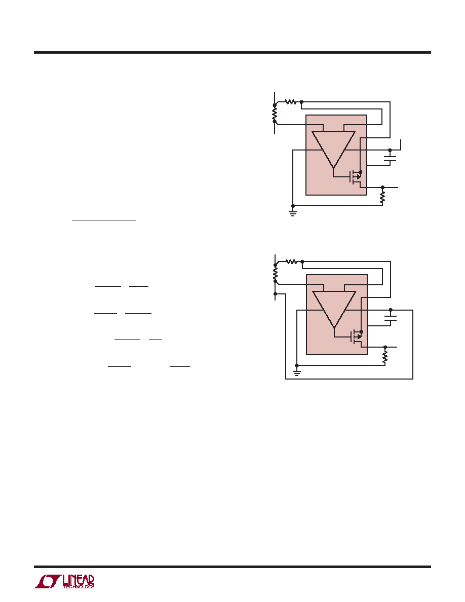
Figure 6. V+ Powered Separately from Load Supply (VBAT)
6102 F06
LTC6102
ROUT
VOUT
RIN
VBAT
LOAD
(V+ – 2V) TO V+
RSENSE
V+
V–
OUT
+IN
V+
–INF
–INS
VREG
0.1μF
–
+
APPLICATIONS INFORMATION
Output Filtering
The output voltage, VOUT, is simply IOUT ZOUT. This
makes ltering straightforward. Any circuit may be used
which generates the required ZOUT to get the desired lter
response. For example, a capacitor in parallel with ROUT
will give a low pass response. This will reduce unwanted
noise from the output, and may also be useful as a charge
reservoir to keep the output steady while driving a switch-
ing circuit such as a mux or ADC. This output capacitor
in parallel with an output resistor will create a pole in the
output response at:
f
RC
dB
OUT
–
3
1
2
=
π
Useful Equations
Input Voltage: V
Voltage
SENSE = IR
SENSE
G
Gain:
V
Current Gain:
I
OUT
SENSE
OUT
S
=
R
OUT
IN
E
ENSE
OUT
SENSE
Transconductance:
I
V
=
R
SENSE
IN
1
R
IN
SENSE
OUT
Transimpedance:
V
I
OUT
SENSE
=
IIN
Input Sense Range
The inputs of the LTC6102 can function from V+ to (V+ – 2V).
Not only does this allow a wide VSENSE range, it also allows
the input reference to be separate from the positive supply
(Figure 6). Note that the difference between VBAT and V+
must be no more than the input sense voltage range listed
in the Electrical Characteristics table.
Monitoring Voltages Above V+ and Level Translation
The LTC6102 may be congured to monitor voltages that are
higher than its supply, provided that the negative terminal
of the input voltage is within the input sense range of the
LTC6102. Figure 7 illustrates a circuit in which the LTC6102
has its supply pin tied to the lower potential terminal of the
sense resistor instead of the higher potential terminal. The
Figure 7. LTC6102 Supply Current Monitored with Load
–INF
–INS
LTC6102
ROUT
VOUT
6102 F07
RIN
LOAD
VBAT
RSENSE
V+
V–
OUT
+IN
VREG
0.1 F
–
+
operation of the LTC6102 is such that the –INS and –INF
pins will servo to within a few microvolts of +IN, which is
shorted to V+. Since the input sense range of the LTC6102
includes V+, the circuit will operate properly. The voltage
across RSENSE will be held across RIN by the LTC6102,
causing current VSENSE/RIN to ow to ROUT. In this case,
the supply current of the LTC6102 is also monitored, as
it ows through RSENSE.
Because the voltage across RSENSE is not restricted to
the sense range of the LTC6102 in this circuit, VSENSE
can be large compared to the allowed sense voltage. This
facilitates the sensing of very large voltages, provided
that RIN is chosen so that VSENSE/RIN does not exceed
相关PDF资料 |
PDF描述 |
|---|---|
| VA100014A300DL | VARISTOR TVS 14VDC 40A AXIAL |
| 2-535541-0 | CONN RCPT 22POS VERT .100 GOLD |
| VA100005A150DL | VARISTOR TVS 5.6VDC 40A AXIAL |
| 1-87987-0 | 10 MODI BDMNT RCPT SR .156CL |
| 1-87985-0 | CONN RCPT 10POS VERT .156 PCB |
相关代理商/技术参数 |
参数描述 |
|---|---|
| LTC6102HDD-PBF | 制造商:LINER 制造商全称:Linear Technology 功能描述:Precision Zero Drift Current Sense Amplifi er |
| LTC6102HDD-TR | 制造商:LINER 制造商全称:Linear Technology 功能描述:Precision Zero Drift Current Sense Amplifi er |
| LTC6102HDD-TRPBF | 制造商:LINER 制造商全称:Linear Technology 功能描述:Precision Zero Drift Current Sense Amplifi er |
| LTC6102HMS#PBF | 制造商:Linear Technology 功能描述:AMP CURRENT SENSE PRECISION SMD |
| LTC6102HMS8 | 制造商:Linear Technology 功能描述:SP Amp Current Sense Amp Single 60V 8-Pin MSOP |
发布紧急采购,3分钟左右您将得到回复。