- 您现在的位置:买卖IC网 > PDF目录5793 > LTC1051CSW#TR (Linear Technology)IC OPAMP CHOP STABLE DUAL 16SOIC PDF资料下载
参数资料
| 型号: | LTC1051CSW#TR |
| 厂商: | Linear Technology |
| 文件页数: | 14/16页 |
| 文件大小: | 0K |
| 描述: | IC OPAMP CHOP STABLE DUAL 16SOIC |
| 标准包装: | 1,000 |
| 放大器类型: | 断路器(零漂移) |
| 电路数: | 2 |
| 转换速率: | 4 V/µs |
| 增益带宽积: | 2.5MHz |
| 电流 - 输入偏压: | 15pA |
| 电压 - 输入偏移: | 0.5µV |
| 电流 - 电源: | 1mA |
| 电压 - 电源,单路/双路(±): | 4.75 V ~ 16 V,±2.38 V ~ 8 V |
| 工作温度: | 0°C ~ 70°C |
| 安装类型: | 表面贴装 |
| 封装/外壳: | 16-SOIC(0.295",7.50mm 宽) |
| 供应商设备封装: | 16-SO |
| 包装: | 带卷 (TR) |
7
LTC1051/LTC1053
10513fa
As the ambient temperature rises, the leakage current of
the input protection devices increases, while the charge
injection component of the bias current, for all practical
purposes, stays constant. At elevated temperatures (above
85°C) the leakage current dominates and the bias current
of both inputs assumes the same sign.
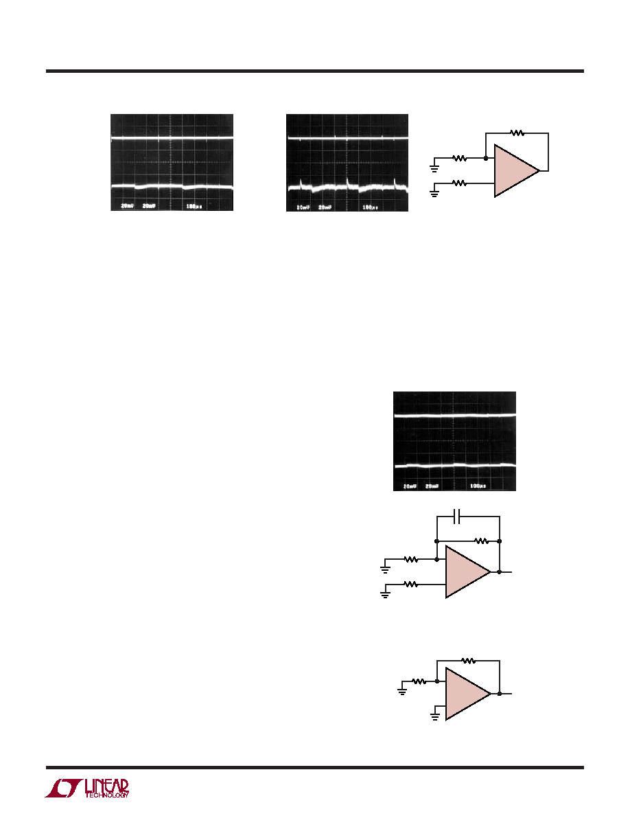
The charge injection at the op amp input pins will cause
small output spikes. This phenomenon is often referred to
as “clock feedthrough” and can be easily observed when
the closed-loop gain exceeds 10V/V (Figure 2). The mag-
nitude of the clock feedthrough is temperature indepen-
dent but it increases when the closed-loop gain goes up,
when the source resistance increases and when the gain
setting resistors increase (Figure 2a, 2b). It is important to
note that the output small spikes are centered at 0V level
and do not add to the output offset error budget. For
instance, with RS = 1M, the typical output offset voltage
of Figure 2c is:
VOS(OUT) ≈ 108 IB+ + 101VOS(IN)
A 10pA bias current will yield an output of 1mV ±100V.
The output clock feedthrough can be attenuated by lower-
ing the value of the gain setting resistors, i.e. R2 = 10k,
R1 = 100, instead of 100k and 1k (Figure 2).
Clock feedthrough can also be attenuated by adding a
capacitor across the feedback resistor to limit the circuit
bandwidth below the internal sampling frequency
(Figure 3).
Input Capacitance
The input capacitance of the LTC1051/LTC1053 op amps
is approximately 12pF. When the LTC1051/LTC1053 op
amps are used with feedback factors approaching unity,
the feedback resistor value should not exceed 7k for
industrial temperature range and 5k for military tempera-
ture range. If a higher feedback resistor value is required,
a feedback capacitor of 20pF should be placed across the
feedback resistor. Note that the most common circuits
with feedback factors approaching unity are unity gain
followers and instrumentation amplifier front ends.
(See Figure 4.)
Figure 2. Clock Feedthrough
Figure 3. Adding a Feedback Capacitor to
Eliminate Clock Feedthrough
–
+
1/2
LTC1051
RS
1051/53 F02
(c)
100s/DIV
(b)
100s/DIV
(a)
R1
1k
R2
100k
RS = 0,
AV =11V/V
20mV/DIV
RS = 0,
AV =101V/V
20mV/DIV
RS = 100k,
AV =11V/V
20mV/DIV
RS = 100k,
AV =101V/V
20mV/DIV
Figure 4. Operating the LTC1051
with Feedback Factors Approaching Unity
–
+
1/2
LTC1051
1051/53 F04
R1
R2 < 7k, IF R1 > >R2
1
2
3
–
+
1/2
LTC1051
RS
1051/53 F03
R1
1k
R2
100k
C
1000pF
1
2
3
100s/DIV
RS = 100k
AV =101V/V
RS = 1M
AV =101V/V
20mV/DIV
APPLICATIO S I FOR ATIO
WU
UU
相关PDF资料 |
PDF描述 |
|---|---|
| 1445054-9 | CONN HEADER 9POS R/A TIN T/H |
| 2026-15-CB | GAS DISCHARGE TUBE 3 POLE |
| 1445054-8 | CONN HEADER 8POS R/A TIN T/H |
| 1445054-7 | CONN HEADER 7POS R/A TIN T/H |
| 1445054-6 | CONN HEADER 6POS R/A TIN T/H |
相关代理商/技术参数 |
参数描述 |
|---|---|
| LTC1051M | 制造商:LINER 制造商全称:Linear Technology 功能描述:Dual/Quad Precision Chopper Stabilized Operational Amplifiers with Internal Capacitors |
| LTC1051MJ8 | 制造商:LINER 制造商全称:Linear Technology 功能描述:Dual/Quad Precision Chopper Stabilized Operational Amplifiers with Internal Capacitors |
| LTC1051MJ8/883 | 制造商:Linear Technology 功能描述:OP Amp Dual Chopper/Stable ±8.25V/16.5V 8-Pin CDIP 制造商:Linear Technology 功能描述:OP Amp Dual Chopper/Stable }8.25V/16.5V 8-Pin CDIP |
| LTC1052 | 制造商:LINER 制造商全称:Linear Technology 功能描述:Chopper-Stabilized Operational Amplifier(CSOATM) |
| LTC1052_09 | 制造商:LINER 制造商全称:Linear Technology 功能描述:Zero-Drift Operational Amplifier |
发布紧急采购,3分钟左右您将得到回复。