参数资料
| 型号: | LT6200CS8-5#PBF |
| 厂商: | Linear Technology |
| 文件页数: | 20/26页 |
| 文件大小: | 0K |
| 描述: | IC OPAMP R-R I/O 800MHZ 8SOIC |
| 标准包装: | 100 |
| 放大器类型: | 缓冲器 |
| 电路数: | 1 |
| 输出类型: | 满摆幅 |
| 转换速率: | 250 V/µs |
| 增益带宽积: | 800MHz |
| 电流 - 输入偏压: | 23µA |
| 电压 - 输入偏移: | 2500µV |
| 电流 - 电源: | 20mA |
| 电流 - 输出 / 通道: | 90mA |
| 电压 - 电源,单路/双路(±): | 2.5 V ~ 12.6 V,±1.25 V ~ 6.3 V |
| 工作温度: | 0°C ~ 70°C |
| 安装类型: | 表面贴装 |
| 封装/外壳: | 8-SOIC(0.154",3.90mm 宽) |
| 供应商设备封装: | 8-SO |
| 包装: | 管件 |
3
62001ff
LT6200/LT6200-5
LT6200-10/LT6201
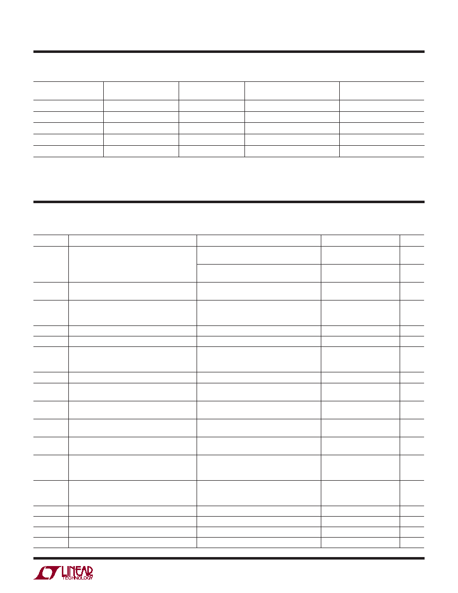
LEAD FREE FINISH
TAPE AND REEL
PART MARKING*
PACKAGE DESCRIPTION
SPECIFIED
TEMPERATURE RANGE
LT6200CS8-10#PBF
LT6200CS8-10#TRPBF
620010
8-Lead Plastic SO
0°C to 70°C
LT6200IS8-10#PBF
LT6200IS8-10#TRPBF
200I10
8-Lead Plastic SO
–40°C to 85°C
LT6201CDD#PBF
LT6201CDD #TRPBF
LADG
8-Lead (3mm
× 3mm) Plastic DFN 0°C to 70°C
LT6201CS8#PBF
LT6201CS8 #TRPBF
6201
8-Lead Plastic SO
0°C to 70°C
LT6201IS8 #PBF
LT6201IS8 #TRPBF
6201I
8-Lead Plastic SO
–40°C to 85°C
Consult LTC Marketing for parts specified with wider operating temperature ranges. *The temperature grade is identified by a label on the shipping container.
Consult LTC Marketing for information on non-standard lead based finish parts.
For more information on lead free part marking, go to: http://www.linear.com/leadfree/
For more information on tape and reel specifications, go to: http://www.linear.com/tapeandreel/
orDer inForMaTion
elecTrical characTerisTics
SYMBOL
PARAMETER
CONDITIONS
MIN
TYP
MAX
UNITS
VOS
Input Offset Voltage
VS = 5V, VCM = Half Supply
VS = 3V, VCM = Half Supply
0.1
0.9
1
2.5
mV
VS = 5V, VCM = V+ to V –
VS = 3V, VCM = V+ to V –
0.6
1.8
2
4
mV
Input Offset Voltage Match
(Channel-to-Channel) (Note 11)
VCM = Half Supply
VCM = V– to V+
0.2
0.5
1.1
2.2
mV
IB
Input Bias Current
VCM = Half Supply
VCM = V+
VCM = V–
–40
–50
–10
8
–23
18
A
IB
IB Shift
VCM = V– to V+
31
68
A
IB Match (Channel-to-Channel) (Note 11)
VCM = V– to V+
0.3
5
A
IOS
Input Offset Current
VCM = Half Supply
VCM = V+
VCM = V–
0.1
0.02
0.4
4
5
A
Input Noise Voltage
0.1Hz to 10Hz
600
nVP-P
en
Input Noise Voltage Density
f = 100kHz, VS = 5V
f = 10kHz, VS = 5V
1.1
1.5
2.4
nV/√Hz
in
Input Noise Current Density, Balanced Source
Unbalanced Source
f = 10kHz, VS = 5V
2.2
3.5
pA/√Hz
Input Resistance
Common Mode
Differential Mode
0.57
2.1
MΩ
kΩ
CIN
Input Capacitance
Common Mode
Differential Mode
3.1
4.2
pF
AVOL
Large-Signal Gain
VS = 5V, VO = 0.5V to 4.5V, RL = 1k to VS/2
VS = 5V, VO = 1V to 4V, RL = 100Ω to VS/2
VS = 3V, VO = 0.5V to 2.5V, RL = 1k to VS/2
70
11
17
120
18
70
V/mV
CMRR
Common Mode Rejection Ratio
VS = 5V, VCM = V– to V+
VS = 5V, VCM = 1.5V to 3.5V
VS = 3V, VCM = V– to V+
65
85
60
90
112
85
dB
CMRR Match (Channel-to-Channel) (Note 11)
VS = 5V, VCM = 1.5V to 3.5V
80
105
dB
PSRR
Power Supply Rejection Ratio
VS = 2.5V to 10V, LT6201DD VS = 2.5V to 7V
60
68
dB
PSRR Match (Channel-to-Channel) (Note 11)
VS = 2.5V to 10V, LT6201DD VS = 2.5V to 7V
65
100
dB
Minimum Supply Voltage (Note 6)
2.5
V
TA = 25°C, VS = 5V, 0V; VS = 3V, 0V; VCM = VOUT = half supply, VSHDN = OPEN,
unless otherwise noted.
相关PDF资料 |
PDF描述 |
|---|---|
| MMA21-0341QU | CONN RACK/PANEL 34POS 5A |
| 966204-2000-AR-PR | CONN SOCKET LO-PRO 4PS GOLD SMD |
| NPTC041KFXC-RC | CONN FEMALE 4POS .1" SMD TIN |
| 963104-2000-AR-PR | CONN SOCKET SGL 4POS GOLD SMD |
| LT1077CN8 | IC PREC OP-AMP MICRPWR SNGL 8DIP |
相关代理商/技术参数 |
参数描述 |
|---|---|
| LT6200CS8-5TRPBF | 制造商:LINER 制造商全称:Linear Technology 功能描述:165MHz, Rail-to-Rail Input and Output, 0.95nV/√Hz Low Noise, Op Amp Family |
| LT6200CS8PBF | 制造商:Linear Technology 功能描述:LT6200 165MHz ULN SOIC op amp |
| LT6200CS8TRPBF | 制造商:LINER 制造商全称:Linear Technology 功能描述:165MHz, Rail-to-Rail Input and Output, 0.95nV/√Hz Low Noise, Op Amp Family |
| LT6200IS6 | 制造商:Linear Technology 功能描述:OP Amp Single GP R-R I/O ±6.3V/12.6V 6-Pin TSOT-23 |
| LT6200IS6#PBF | 制造商:Linear 功能描述:ic smt 制造商:Linear Technology 功能描述:SC-Amps/High Speed, Cut Tape 165MHz, Ultra Low Noise, RR OA |
发布紧急采购,3分钟左右您将得到回复。