- 您现在的位置:买卖IC网 > PDF目录19364 > LT3466EFE#PBF (Linear Technology)IC LED DRVR WHITE BCKLGT 16TSSOP PDF资料下载
参数资料
| 型号: | LT3466EFE#PBF |
| 厂商: | Linear Technology |
| 文件页数: | 8/20页 |
| 文件大小: | 0K |
| 描述: | IC LED DRVR WHITE BCKLGT 16TSSOP |
| 标准包装: | 95 |
| 恒定电流: | 是 |
| 拓扑: | PWM,升压(升压) |
| 输出数: | 2 |
| 内部驱动器: | 是 |
| 类型 - 主要: | 车载,背光 |
| 类型 - 次要: | 白色 LED |
| 频率: | 800kHz ~ 1.3MHz |
| 电源电压: | 2.7 V ~ 24 V |
| 输出电压: | 39.5V |
| 安装类型: | 表面贴装 |
| 封装/外壳: | 16-TSSOP(0.173",4.40mm)裸露焊盘 |
| 供应商设备封装: | 16-TSSOP-EP |
| 包装: | 管件 |
| 工作温度: | -40°C ~ 85°C |
�� �
�
�LT3466�
�OPERATIO�
�Main� Control� Loop�
�The� LT3466� uses� a� constant� frequency,� current� mode�
�control� scheme� to� provide� excellent� line� and� load� regula-�
�tion.� It� incorporates� two� identical,� but� fully� independent�
�PWM� converters.� Operation� can� be� best� understood� by�
�referring� to� the� Block� Diagram� in� Figure� 2.� The� oscillator,�
�start-up� bias� and� the� bandgap� reference� are� shared� be-�
�tween� the� two� converters.� The� control� circuitry,� power�
�switch,� Schottky� diode� etc.,� are� all� identical� for� both� the�
�converters.�
�At� power-up,� the� output� voltages� V� OUT1� and� V� OUT2� are�
�charged� up� to� V� IN� (input� supply� voltage)� via� their� respec-�
�tive� inductor� and� the� internal� Schottky� diode.� If� either�
�CTRL1� and� CTRL2� or� both� are� pulled� high,� the� bandgap�
�reference,� start-up� bias� and� the� oscillator� are� turned� on.�
�Working� of� the� main� control� loop� can� be� understood� by�
�following� the� operation� of� converter� 1.� At� the� start� of� each�
�oscillator� cycle,� the� power� switch� Q1� is� turned� on.� A�
�voltage� proportional� to� the� switch� current� is� added� to� a�
�stabilizing� ramp� and� the� resulting� sum� is� fed� into� the�
�positive� terminal� of� the� PWM� comparator� A2.� When� this�
�result� in� some� low� frequency� ripple,� although� the� LED�
�current� remains� regulated� on� an� average� basis� down� to�
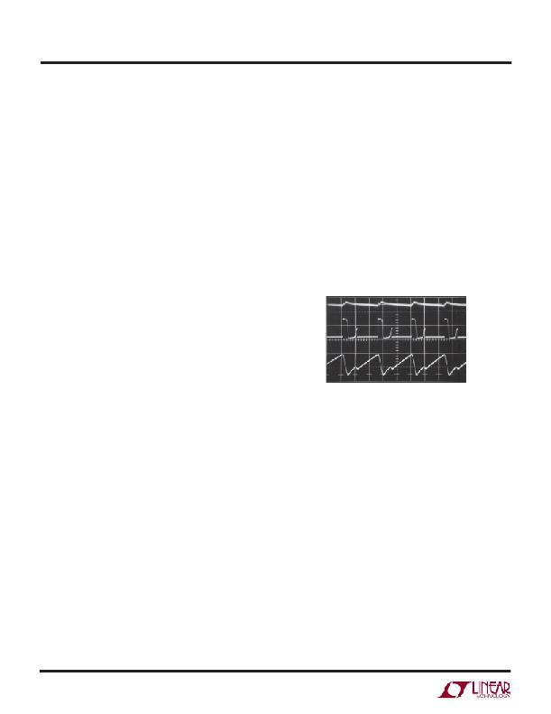
�zero.� The� photo� in� Figure� 3� shows� circuit� operation� with� 16�
�white� LEDs� (eight� per� converter)� at� 2.5mA� current� driven�
�from� 3.6V� supply.� Peak� inductor� current� is� less� than� 50mA�
�and� the� regulator� operates� in� discontinuous� mode� imply-�
�ing� that� the� inductor� current� reached� zero� during� the�
�discharge� phase.� After� the� inductor� current� reaches� zero,�
�the� switch� pin� exhibits� ringing� due� to� the� LC� tank� circuit�
�formed� by� the� inductor� in� combination� with� switch� and�
�diode� capacitance.� This� ringing� is� not� harmful;� far� less�
�spectral� energy� is� contained� in� the� ringing� than� in� the�
�switch� transitions.� The� ringing� can� be� damped� by� applica-�
�tion� of� a� 300� ?� resistor� across� the� inductors,� although� this�
�will� degrade� efficiency.�
�V� OUT1�
�10mV/DIV�
�V� SW1�
�20V/DIV�
�I� L1�
�50mA/DIV�
�voltage� exceeds� the� level� at� the� negative� input� of� A2,� the�
�PWM� logic� turns� off� the� power� switch.� The� level� at� the�
�negative� input� of� A2� is� set� by� the� error� amplifier� A1,� and� is�
�simply� an� amplified� version� of� the� difference� between� the�
�feedback� voltage� and� the� 200mV� reference� voltage.� In� this�
�V� IN� =� 3.6V� 0.5� μ� s/DIV�
�I� LED1� =� 2.5mA�
�CIRCUIT� OF� FIGURE� 1�
�Figure� 3.� Switching� Waveforms�
�3466� F03�
�manner,� the� error� amplifier� A1� regulates� the� feedback�
�voltage� to� 200mV� reference� voltage.� The� output� of� the�
�error� amplifier� A1� sets� the� correct� peak� current� level� in�
�inductor� L1� to� keep� the� output� in� regulation.� The� CTRL1�
�pin� voltage� is� used� to� adjust� the� reference� voltage.�
�If� only� one� of� the� converters� is� turned� on,� the� other� con-�
�verter� will� stay� off� and� its� output� will� remain� charged� up� to�
�V� IN� (input� supply� voltage).� The� LT3466� enters� into� shut-�
�down,� when� both� CTRL1� and� CTRL2� are� pulled� lower� than�
�50mV.� The� CTRL1� and� CTRL2� pins� perform� independent�
�dimming� and� shutdown� control� for� the� two� converters.�
�Minimum� Output� Current�
�The� LT3466� can� drive� an� 8-LED� string� at� 2.5mA� LED�
�current� without� pulse� skipping.� As� current� is� further�
�reduced,� the� device� may� begin� skipping� pulses.� This� will�
�Open-Circuit� Protection�
�The� LT3466� has� internal� open-circuit� protection� for� both�
�the� converters.� When� the� LEDs� are� disconnected� from� the�
�circuit� or� fail� open,� the� converter� output� voltage� is� clamped�
�at� 39.5V� (typ).� Figure� 4a� shows� the� transient� response� of�
�Figure� 1’s� step-up� converter� with� LED1� disconnected.�
�With� LED1� disconnected,� the� converter� starts� switching� at�
�the� peak� inductor� current� limit.� The� converter� output� starts�
�ramping� up� and� finally� gets� clamped� at� 39.5V� (typ).� The�
�converter� will� then� switch� at� low� inductor� current� to�
�regulate� the� converter� output� at� the� clamp� voltage.� Output�
�voltage� and� input� current� during� output� open� circuit� are�
�shown� in� the� Typical� Performance� Characteristics� graphs.�
�In� the� event� one� of� the� converters� has� an� output� open-�
�circuit,� its� output� voltage� will� be� clamped� at� 39.5V.�
�3466fa�
�8�
�相关PDF资料 |
PDF描述 |
|---|---|
| TAJY686M020RNJ | CAP TANT 68UF 20V 20% 2917 |
| TAP476M016HSB | CAP TANT 47UF 16V 20% RADIAL |
| DBMF25S | CONN DSUB RCPT 25POS SLD CUP POS |
| RMA36DRMZ-S664 | CONN EDGECARD 72POS .125 SQ WW |
| FAN5702UC08X | IC LED DVR 6LED 8MA I2C 16WLCSP |
相关代理商/技术参数 |
参数描述 |
|---|---|
| LT3467 | 制造商:LINER 制造商全称:Linear Technology 功能描述:700mA Low Noise High Current LED Charge Pump |
| LT3467A | 制造商:LINER 制造商全称:Linear Technology 功能描述:700mA Low Noise High Current LED Charge Pump |
| LT3467AEDDB#PBF | 制造商:Linear Technology 功能描述:SP-SWREG/Monolithic, Cut Tape 1.1A, 2.1MHz Boost Converter |
| LT3467AEDDB#TRMPBF | 功能描述:IC REG BOOST ADJ 1.1A 8DFN RoHS:是 类别:集成电路 (IC) >> PMIC - 稳压器 - DC DC 开关稳压器 系列:- 标准包装:2,500 系列:- 类型:升压(升压) 输出类型:可调式 输出数:1 输出电压:1.24 V ~ 30 V 输入电压:1.5 V ~ 12 V PWM 型:电流模式,混合 频率 - 开关:600kHz 电流 - 输出:500mA 同步整流器:无 工作温度:-40°C ~ 85°C 安装类型:表面贴装 封装/外壳:8-SOIC(0.154",3.90mm 宽) 包装:带卷 (TR) 供应商设备封装:8-SOIC |
| LT3467AEDDB#TRPBF | 功能描述:IC REG BOOST ADJ 1.1A 8DFN RoHS:是 类别:集成电路 (IC) >> PMIC - 稳压器 - DC DC 开关稳压器 系列:- 标准包装:2,500 系列:- 类型:升压(升压) 输出类型:可调式 输出数:1 输出电压:1.24 V ~ 30 V 输入电压:1.5 V ~ 12 V PWM 型:电流模式,混合 频率 - 开关:600kHz 电流 - 输出:500mA 同步整流器:无 工作温度:-40°C ~ 85°C 安装类型:表面贴装 封装/外壳:8-SOIC(0.154",3.90mm 宽) 包装:带卷 (TR) 供应商设备封装:8-SOIC |
发布紧急采购,3分钟左右您将得到回复。