- 您现在的位置:买卖IC网 > PDF目录15903 > C8051F206DK-U (Silicon Laboratories Inc)DEV KIT FOR C8051F206 PDF资料下载
参数资料
| 型号: | C8051F206DK-U |
| 厂商: | Silicon Laboratories Inc |
| 文件页数: | 7/12页 |
| 文件大小: | 0K |
| 描述: | DEV KIT FOR C8051F206 |
| 标准包装: | 1 |
| 其它名称: | 336-1040 |
�� �
�
�C8051F2xx-DK�
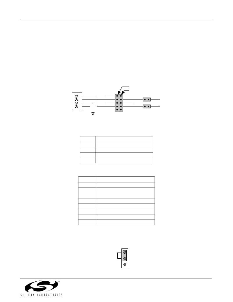
�6.4.� Analog� I/O� (J5,� J6,� J7,� Terminal� Block)�
�An� Analog� I/O� Configuration� connector� (J6)� provides� the� ability� to� route� analog� I/O� signals� from� the� C8051F2xx� to�
�a� terminal� block� in� addition� to� connector� J2� by� installing� shorting� blocks� on� J6.� Additionally,� if� shorting� blocks� are�
�installed� on� J5� and� J7,� the� analog� signals� routed� through� J6� can� be� inputs� to� the� C8051F2xx� at� port� pins� P3.0�
�and/or� P3.1.� The� port� pins� can� then� be� configured� as� inputs� to� the� on-chip� ADC� for� evaluation.� J6� also� allows� the�
�user� to� route� analog� signals� from� the� terminal� block� to� port� pins� P1.3� and� P1.4.� These� port� pin� can� then� be�
�configured� as� inputs� to� Comparator� 1.� The� PWM� signal� from� the� low-pass� filter� is� also� routed� to� J6� to� provide� a�
�user� controlled� analog� voltage� level.� This� signal� can� then� be� used� to� evaluate� the� on-chip� ADC� by� placing� a�
�shorting� block� on� J6� (provided� the� J5� or� J7� header� is� shorted).� Refer� to� Figure� 3� to� determine� the� shorting� block�
�installation� positions� required� to� create� the� desired� analog� signal� paths.� Refer� to� Table� 3� for� terminal� block�
�connections� and� Table� 4� for� J6� pin� definitions.�
�Pin� 1�
�Pin� 2�
�AIN1�
�AIN2�
�GND�
�Vref�
�P1.4/CP1-�
�AIN2�
�P1.3/CP1+�
�AIN1�
�P3.0AIN�
�PWM�
�P3.1AIN�
�J5�
�P3.0�
�P3.1�
�J7�
�J6�
�Figure� 3.� J6� Analog� I/O� Configuration� Connector�
�Table� 3.� Terminal� Block� Pin� Descriptions�
�Pin� #�
�1�
�2�
�7�
�8�
�Description�
�VREF�
�GND�
�AIN2�
�AIN1�
�Table� 4.� J6� Connector� Pin� Descriptions�
�Pin� #�
�1�
�2,� 9,� 10�
�3�
�4�
�5�
�6�
�7�
�8�
�Description�
�P1.4/CP1-�
�NC�
�AIN2�
�P3.0AIN�
�P1.3/CP1+�
�PWM�
�AIN1�
�P3.1AIN�
�6.5.� VDD� Monitor� Disable� (J1)�
�The� VDD� Monitor� of� the� C8051F2xx� may� be� disabled� by� moving� the� shorting� block� on� J1� from� pins� 1-2� to� pins� 2-3,�
��MONEN�
�1�
�2�
�3�
�Figure� 4.� VDD� Monitor� Hardware� Setup�
�Rev.� 0.6�
�7�
�相关PDF资料 |
PDF描述 |
|---|---|
| M3DRK-6036R | IDC CABLE - MKR60K/MC60M/MPR60K |
| ESM15DSES-S243 | CONN EDGECARD 30POS .156 EYELET |
| C8051F020DK-U | DEV KIT FOR F020/F021/F022/F023 |
| RSM08DTBN-S189 | CONN EDGECARD 16POS R/A .156 SLD |
| RP15-2405SF/P-HC | CONV DC/DC 15W 18-36VIN 05VOUT |
相关代理商/技术参数 |
参数描述 |
|---|---|
| C8051F206-GQ | 功能描述:8位微控制器 -MCU 8KB 12ADC 1KRam 48P MCU RoHS:否 制造商:Silicon Labs 核心:8051 处理器系列:C8051F39x 数据总线宽度:8 bit 最大时钟频率:50 MHz 程序存储器大小:16 KB 数据 RAM 大小:1 KB 片上 ADC:Yes 工作电源电压:1.8 V to 3.6 V 工作温度范围:- 40 C to + 105 C 封装 / 箱体:QFN-20 安装风格:SMD/SMT |
| C8051F206-GQR | 功能描述:8位微控制器 -MCU 8KB 12ADC 1KRam 48P Tape and Reel RoHS:否 制造商:Silicon Labs 核心:8051 处理器系列:C8051F39x 数据总线宽度:8 bit 最大时钟频率:50 MHz 程序存储器大小:16 KB 数据 RAM 大小:1 KB 片上 ADC:Yes 工作电源电压:1.8 V to 3.6 V 工作温度范围:- 40 C to + 105 C 封装 / 箱体:QFN-20 安装风格:SMD/SMT |
| C8051F206R | 功能描述:8位微控制器 -MCU T-121280 Ram 48Pin RoHS:否 制造商:Silicon Labs 核心:8051 处理器系列:C8051F39x 数据总线宽度:8 bit 最大时钟频率:50 MHz 程序存储器大小:16 KB 数据 RAM 大小:1 KB 片上 ADC:Yes 工作电源电压:1.8 V to 3.6 V 工作温度范围:- 40 C to + 105 C 封装 / 箱体:QFN-20 安装风格:SMD/SMT |
| C8051F206-TB | 功能描述:插座和适配器 With C8051F206 MCU RoHS:否 制造商:Silicon Labs 产品:Adapter 用于:EM35x |
| C8051F220 | 功能描述:8位微控制器 -MCU 8KB 8ADC RoHS:否 制造商:Silicon Labs 核心:8051 处理器系列:C8051F39x 数据总线宽度:8 bit 最大时钟频率:50 MHz 程序存储器大小:16 KB 数据 RAM 大小:1 KB 片上 ADC:Yes 工作电源电压:1.8 V to 3.6 V 工作温度范围:- 40 C to + 105 C 封装 / 箱体:QFN-20 安装风格:SMD/SMT |
发布紧急采购,3分钟左右您将得到回复。